Recently, in the online edition of Science, Laura M. Herz of the University of Oxford in the United Kingdom and others published a major breakthrough in the atomic crystal structure of hybrid perovskite thin films. The team developed a new imaging technique to obtain the first atomic-level resolution images of the cubic phase FAPbI3 perovskite film. This discovery provides an unprecedented understanding of hybrid perovskites at the atomic level!

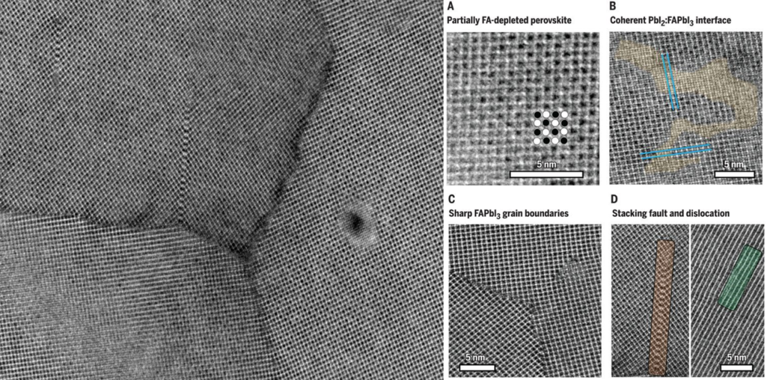
Figure 1: Atomic level resolution image of cubic FAPbI3 perovskite film. The diagram shows several phenomena that the team was able to describe for the first time, including a range of grain boundaries, extended planar imperfections, stacking faults, and local inclusions in non-perovskite materials.
Challenges in the field of polycrystalline hybrid perovskite films
Polycrystalline hybrid metal halide perovskite (MHPs) films have become ideal materials for efficient photovoltaic and photovoltaic applications such as solar cells due to their high optical absorption coefficient, high carrier mobility, surprising regeneration capacity and benign grain boundaries (virtually free of strain and dislocation). Although hybrid MHP solar cells have made great progress in recent years, the mechanism behind their impressive performance is not fully understood. Although it has been speculated that its excellent performance may depend on unique atomic properties, the structure of the MHP polycrystalline interface and the exact atomic properties of the grain boundaries are not yet described. Even the technically important formamidine lead perovskite (FAPbI3) MHP has not yet been crystallized.

In recent years, atomic resolution transmission electron microscopy (TEM) has successfully performed atomic resolution imaging of all inorganic photoperovskite. However, due to the high beam sensitivity of the hybrid perovskite film, it is extremely unstable under the electron beam. Even under mild electron irradiation, MHP will quickly transform into a more stable PbI2 phase. Therefore, observing the microstructure of natural hybrid perovskite films by TEM is still a great challenge in the field of perovskite solar cells. Until now, no atomic resolution images of natural hybrid perovskite films have been reported.
Breakthrough! Unraveling the mystery of the crystal structure of FAPbI3 atoms
In view of this, Laura M. Herz, Department of Physics, University of Oxford, UK, and Peter D. Nellist, Department of Materials, et al. developed a new technique to obtain reliable atomic resolution images of FAPbI3 polycrystalline films for the first time. By using low electron dose scanning transmission electron microscopy and advanced image processing techniques, the researchers not only obtained the atomic crystal structure of FAPbI3 polycrystalline thin films, but also described the exact atomic properties of grain boundaries for the first time.
This technology is revolutionary and has important implications for:
1. Enable them to observe completely new phenomena related to hybrid perovskite multistage films, including important properties, such as the precise composition of grain boundaries and other interfaces, which cannot be achieved with other technologies.
2. Provide an understanding of the atomic level of technically important hybrid perovskite materials, and reveal the possible mechanism behind their excellent properties;
3. Not only was it able to describe exact atomic level properties and answer questions about the atomic structure of hybrid perovskite, but it also opened the way for the study of many other radiation-sensitive materials.
Analysis of important Achievements
Outcome 1: The atomic resolution images of cubic phase FAPbI3 thin films were obtained for the first time using low dose low Angle circular dark field (LAADF) STEM imaging technology.

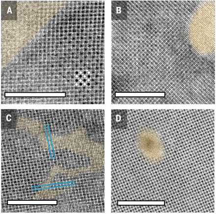
Figure 2: Atomic resolution imaging of metal halide perovskite structure.
It was found that long time electron irradiation would lead to FA+ ion loss, which changed the perovskite structure into a partially FA+ depleted but ordered perovskite lattice. The expected final decomposition product PbI2 degrades with the prolonged exposure time of electron beam. The initial beam induces a FA+ loss, leaving part of the unoccuated perovskite lattice, which is then subsequently reordered by the FA+ ions. The discovery of this intermediate structure explains the surprising ability of perovskite structures to regenerate.
Outcome 2: The atomic arrangement at the grain boundary of the hybrid perovskite film was revealed: highly ordered atomic arrangement at the coherent perovskite/PbI2 interface, with no obvious distant disorder in the crystal.

Figure 3: Atomic resolution LAADF photomicrograph of the FAPbI3 film, showing the transition between PbI2 and FAPbI3 without distortion, and the grid strength after minor radiation damage.
It is found that the common precursors of PbI2 in hybrid perovskite films can easily and seamlessly co-exist with FAPbI3 and MAPbI3 lattices, and can deform from its body hexagonal structure to form unexpected coherent transition boundary, showing lower lattice mismatch and strain. Moreover, PbI2 domains almost completely follow the surrounding perovskite structure and orientation, suggesting that PbI2 may be the seed of perovskite growth. These observations help explain why the presence of excess PbI2 tends not to hamper the performance of solar cells.
Outcome 3: The researchers further determined the properties of defects, dislocations and stacking faults in the FAPbI3 lattice, which is of great guiding significance for improving the performance of perovskite materials.

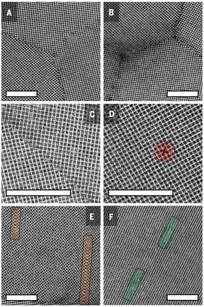
Figure 4: Grain boundaries and crystal defects of FAPbI3 films, atomic resolution LAADF photomicrograph filtered by Butterworth.
The researchers observed a series of crystallographic defects that had significant effects on grain boundaries. Eliminating these defects is important for improving the performance of perovskite solar cells, but until now their existence has not been reliably determined. It is found that in the direction perpendicular to its sliding plane, the dislocations (climbing dislocations), the alignment defects in the form of vacancies on the PB-1 sublattice and the stacking defects connect the PB-I and I-columns together.
"Using our technology, we have been able to describe the exact atomic properties of the grain boundaries, which is one of the most difficult aspects of perovskite solar cells to understand, and to describe a new set of crystal defects that have a significant impact on the grain boundaries. We can say that our findings have opened the door to a new level of understanding of these materials. Although we do not yet fully understand what this means for the development of these solar cells, when trying to answer questions about the microscopic properties of perovskite-type solar cell materials, we will be able to give definitive answers, not just educated guesses. Answering these questions accurately represents a huge step toward better performance in the field." Dr. Rothmann conclud


