Writer | Charlie (PhD student, Zhejiang University)
In recent years, with the booming of a new generation of information industries such as artificial intelligence, big data, and 5G, the amount of data that human society has to process and analyze has also increased day by day. Statistics show that the total amount of global data will reach 44ZB in 2020, and the total amount of global data will reach 175ZB by 2025, an increase of more than three times.These massive amounts of data put increasing demands on the computing power of our chips.
Recently, the Zhou Peng (picture extension link) team of the School of Microelectronics of Fudan University published a review article in Nature Nanotechnology, entitled "Two-dimensional materials for next-generation computing technologies". Focusing on the methods and potentials of applying two-dimensional materials to matrix calculations and logic calculations, it also points out the respective advantages and disadvantages of two-dimensional materials and traditional materials in the future computing chips Prospects for the development of computing technology.

According to different data processing methods, computing tasks can be divided into two types: perception and reasoning.
Typical examples of perceptual computing include neural network-based computing such as image recognition and natural language processing. Specific examples of inference computing include transistor-based computing such as CPU and FPGA.
When dealing with perceptual calculations such as object recognition and natural language processing, the highly parallel matrix calculation method is the best method; while dealing with inference calculation tasks, the serial logic calculation method will be more efficient.
The current computing architecture is a von Neumann-type architecture that physically separates the computing unit and the storage unit. Users can only use this single computing architecture to solve perceptual computing and reasoning computing at the same time. However, the different requirements of perceptual computing and inferential computing on computing architecture pose severe challenges to the von Neumann configuration.
On the one hand, the data transmission rate between the computing unit and the storage unit is limited by the architecture, so that the energy and time consumption of data migration when processing perceptual tasks is even greater than the computing itself. Although the industry has proposed near-memory technology to improve energy efficiency, the constraints of the connection density of through silicon vias make this near-memory technology insufficient to achieve energy-efficient computing.
On the other hand, the improvement of calculation performance for reasoning tasks requires higher transistor density in the logic processing unit. However,when the silicon thickness is reduced below 3nm,
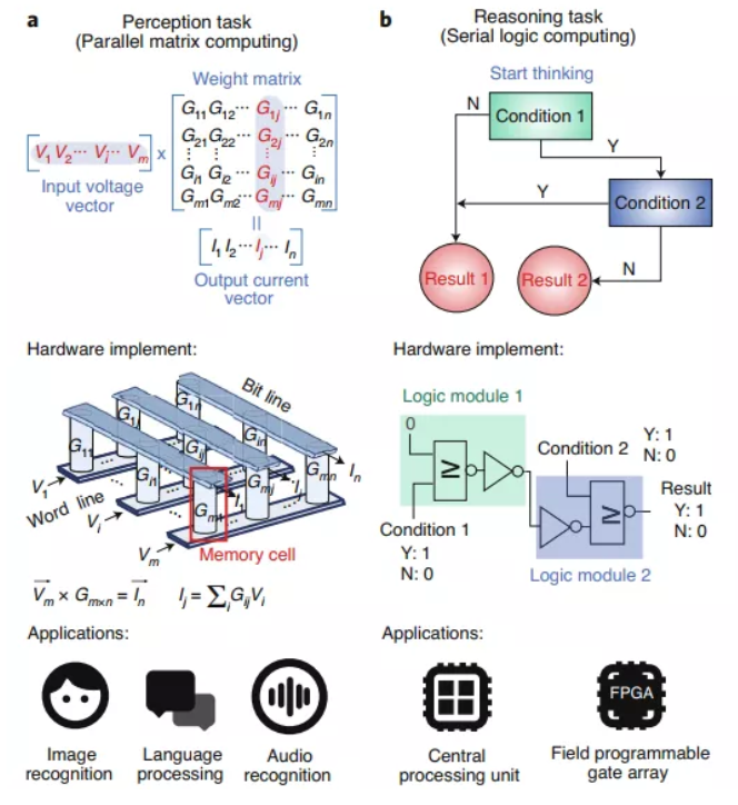
Figure 1 Schematic diagram of matrix operations and logical operations
Image source: Nature Nanotechnology 15, 545-557(2020)(Fig.1)
Later, people realized that, as shown in Figure 1, since perceptual computing and inferential computing have different requirements for architecture, designing different architectures according to different types of computing tasks is a more efficient way to solve computing performance problems. Based on this, people designed in-memory calculations for perceptual computing tasks, and transistor calculations for reasoning computing.
In-memory computing is a technology that uses memory devices arranged in an array to perform matrix operations. This technology can avoid the time and energy consumption caused by data migration. This technology is very promising in matrix operations, but there are still many technical problems to be solved before commercial applications. The operation of the memory will significantly increase the energy consumption of the calculation, which will offset the energy-saving advantage brought by the in-memory calculation itself; and the instability of the memory will reduce the accuracy of the calculation; at the same time, the non-ionic dynamics mechanism will reduce the energy consumption. The actual realization of the bionic system brings many difficulties.
For logic calculations, in-memory calculations have been proven to be inappropriate for serial calculations, because the logic calculation efficiency of in-memory calculations is very low, so field effect transistor technology is still the most promising choice. In order to reduce the characteristic size of the transistor below 5nm, the bulk material will no longer be an optimal material system due to the strong scattering caused by its dangling bonds. The advantage of two-dimensional materials without dangling bonds makes it possible to overcome the size limitations of traditional transistors, while realizing a high-area efficient integrated computing structure that integrates computing and memory.
In this review, the author reviewed the performance improvements and device innovations brought by two-dimensional materials in chip computing, including the reduction of power consumption in in-memory calculations, the improvement of calculation accuracy and bionic characteristics, and the use of transistor technology in logic calculations. The size reduction advantage and high area efficiency integration potential demonstrated in the.
Since the discovery of graphene, various other two-dimensional materials, especially transition metal disulfides (TMDs), have become a research focus. Each layer of the two-dimensional material is covalently connected by a surface without dangling bonds, and the weak Van der Waals force between adjacent layers makes it easy to separate one layer from the two-dimensional crystal or Several floors. These characteristics make two-dimensional materials have very different properties from traditional bulk materials. Thanks to the unique layered structure of the two-dimensional material, the electrons are bound in a very thin plane, so that the electrons can be precisely controlled by the gate voltage. Therefore, two-dimensional materials have the potential to be immune to short-channel effects.
In the post-Moore era, due to the limitations of quantum effects, it is difficult for bulk materials to achieve feature sizes below 5nm, and the atomic-level thickness of two-dimensional materials makes it a natural material candidate.
In addition, two-dimensional materials have a rich material system, including conductor (Graphene), semiconductor (MoS2), and insulator (hBN) systems. At the same time, it is possible to achieve device innovation through energy band control design. In addition, in recent years, research on two-dimensional magnetic materials has gradually increased. All these unique properties of two-dimensional materials can be used to design novel electronic devices. Finally, one can use the stackable properties of two-dimensional materials to create van der Waals heterojunctions, which further expands the richness of two-dimensional material systems.
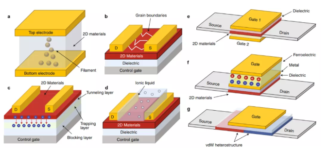
Figure 2 Source of two-dimensional memory devices and two-dimensional transistor devices: Nature Nanotechnology 15, 545-557(2020)(Fig.2)
Memory and transistors are the core devices for realizing in-memory calculations and transistor logic calculations. Two-dimensional materials have great application potential in these two aspects. Two-dimensional memory devices include memristors (Figure 2a), memristive transistors (Figure 2b), flash memory (Figure 2c), and ion transistors (Figure 2d). The memristor uses a classic metal-insulator-metal structure, in which a two-dimensional insulator can be used as an exchange layer. The memristive transistor adopts a three-terminal transistor structure with gate adjustability, and the reversible drift of grain boundary migration or other defects can produce a resistance switching effect.
Flash memory is based on a charge tunneling mechanism, while ion transistors use ion coupling to achieve conductivity modulation. By using these unique properties of two-dimensional materials, memory performance can be greatly improved. For example, two-dimensional atomic crystal graphene can act as a barrier to improve the stability of the device. HBN, which has a honeycomb structure similar to graphene, exhibits completely different high insulation properties. It acts as an exchange layer in the memristor, allowing the memristor to have both high reliability and low programming current.
Because the thickness of the two-dimensional material is very thin, the two-dimensional storage device can use a very low operating voltage to reduce power consumption. In addition, two-dimensional transistors, such as double surface channel (TSC) field effect transistors (Figure 2e), ferroelectric field effect transistors (Figure 2f), or van der Waals heterostructure field effect transistors (Figure 2g) are currently in experiment In the realization. Recent studies have shown that a two-dimensional dual-surface channel FET can be used as a basic logic gate to achieve in-situ storage.
Ferroelectric field effect transistors, such as Negative Capacitance Field Effect Transistors (NCFETs), can realize low-power electronic applications with sub-threshold swings. Furthermore, two-dimensional memory devices can be designed into an array structure to implement matrix operations, and two-dimensional transistors can achieve system-level integration through van der Waals heterojunctions, which is expected to integrate memory and computing.
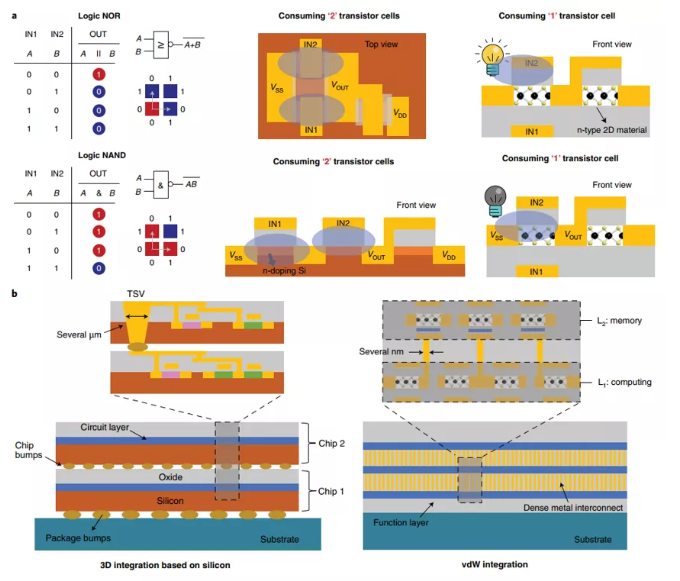
Figure 3 Advantages of two-dimensional material integration
Image source: Nature Nanotechnology 15, 545-557(2020)(Fig. 4)
In addition to improving the performance of a single device, due to the layered structure of the two-dimensional material, the two-dimensional material can achieve a higher area efficiency of the logic gate structure and van der Waals integration, because different kinds of two-dimensional materials can be easily stacked on each other Without considering the limitation of lattice mismatch.
For a chip, logic calculation is realized by a combination of various logic gates. Since either a single NAND gate or a NOR gate can form the entire logic system, the key to the problem is to make a NAND gate or a NOR gate. In the bulk material system, only the surface of the bulk material is used for device design, so at least two transistors are required to assemble the NAND gate or NOR gate (two input ports are required). However, based on two-dimensional materials, researchers proposed a new logic gate structure in 2019, which reduces the transistor resources used to assemble basic logic gates by 50%, and can be realized with only one two-dimensional transistor. Figure 3a shows the comparison between the traditional logic gate design and the logic gate design based on two-dimensional materials.
In a two-dimensional transistor, both the upper and lower surfaces of the channel material can be used; therefore, a two-surface-channel (TSC) two-dimensional transistor can receive enough input signal ports to realize a NAND gate/NOR gate. In addition, the researchers proved that only a single-layer two-dimensional MoS2 transistor connected to a load resistor can realize both a NAND gate and a NOR gate at the same time. At the same time, this logic function can realize a photo switch. Because this two-dimensional transistor can reduce the consumption of transistor resources by 50% and can be flexibly integrated in the vertical direction, this new logic gate structure is worthy of further promotion.
For chip-level integration, vertical integration is the most widely used way to increase chip density, such as near-memory technology. Due to the limitation of lattice defects in bulk materials, traditional three-dimensional integration is achieved through the Through-Silicon-Via (TSV) method, which has very low interconnect density.
Figure 3b shows the comparison between traditional silicon-based 3D integration and van der Waals integration. In silicon-based three-dimensional integration, chips are stacked vertically and connected to each other by the through silicon via method. Considering that the diameter of the hole on the silicon is on the order of a few microns, the efficiency of data migration and the space for chip design are actually very limited. For van der Waals junction integration, we do not need to consider the problem of lattice adaptation. Two-dimensional materials can be grown directly or migrated to the substrate, and excess materials can be etched away. (However, it should be noted that the current direct growth of two-dimensional materials on the substrate is still a very challenging task, and the growth temperature and the quality of the substrate should also be considered.) After the device is manufactured and the oxidative peeling, the second The functional layer can continue to be assembled on the original first functional layer, and the different layers are realized by a few nanometers thick metal passing through the dielectric layer, which is much more efficient than the through silicon via method. Through the use of van der Waals integration method, the interconnection efficiency between adjacent functional layers will no longer be limited. Therefore, each functional layer such as a computing layer and a storage layer can be assembled vertically. Because the computing layer and the storage layer can be interconnected by high-density metal, this method can greatly improve the efficiency of data migration.
Figure 4 Roadmap for the development of two-dimensional materials for the next generation of computing technology Source: Nature Nanotechnology 15, 545-557(2020)(Fig.5)
Thanks to the lattice without dangling bonds and van der Waals heterojunction, two-dimensional materials can improve matrix computing performance, reduce transistor size, improve transistor area efficiency, and have huge advantages in chip integration.
However, in general, the use of two-dimensional materials to perform matrix operations for artificial neural network computing services has just started. Although a research team has recently realized the application of a neural network structure to matrix operations based on two-dimensional materials, the current matrix dimensions are still small. For logic operations, two-dimensional materials have significant advantages in reducing device size and high area efficiency integration. However, there is still a lack of experimental verification of chip-level integration. From the overall perspective of chip development, two-dimensional materials still have some important technical problems to be solved. Specifically, from growing crystals with stable doping in a large area to a reliable method for enhancing chip drive current, to large-scale heterogeneous integration, there are some challenges and difficulties to be solved.
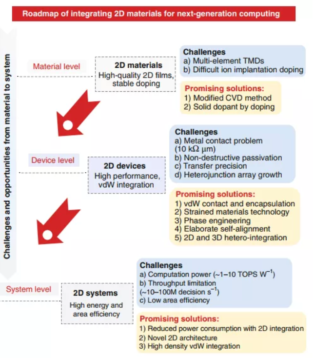
Figure 4 shows the technical roadmap for the development of two-dimensional materials for next-generation computing technologies. From materials to devices to systems, two-dimensional materials not only show unique advantages and potentials, but also propose to our existing technology. Higher requirements and challenges. I believe that if we make unremitting efforts in material growth, device manufacturing and system design, two-dimensional materials will surely play an important role in the next generation of computing technology in the future!
Article information Liu, C., Chen, H., Wang, S. et al. Two-dimensional materials for next-generation computing technologies.Nat. Nanotechnol. 15, 545�C557 (2020).
Paper address https://doi.org/10.1038/s41565-020-0724-3
Source of information: Light Center of Changguang Institute China Optics
This information is from the Internet for academic exchanges. If there is any infringement, please contact us and delete it immediately