Since semiconductor quantum dots have a strong three-dimensional quantum confinement effect, quantum dot (QD) lasers exhibit excellent performance such as low threshold current, high modulation rate, high temperature stability, low linewidth enhancement factor and high anti-reflection. Especially the 1.3 μm InAs/GaAs quantum dot laser, based on its many advantages, can also work without cooling and without optical isolators, thereby greatly reducing cost, energy consumption and device size, and is expected to become the next generation An important light source for optical communication and optical interconnection systems.
In addition, as Moores Law is gradually approaching its limit, silicon-based optoelectronic integration technology has become the direction of future semiconductor technology development. At present, the bottleneck restricting the development of this technology is the lack of efficient silicon-based light sources.
For mass production, direct epitaxy of III-V materials on Si substrates is an ideal technical solution to solve the lack of core light sources for silicon-based optoelectronic integration. Nano-scale zero-dimensional quantum dot structures are not sensitive to dislocations, and are particularly suitable for preparing high-efficiency Si-based III-V semiconductor laser light sources. Therefore, Si-based quantum dot lasers have become another research hotspot in the current semiconductor laser field.
Preparation method of quantum dot material
Quantum dot materials have been used to develop high-performance semiconductor devices, including quantum dot lasers, quantum dot photodetectors, and quantum dot solar cells. In order to obtain quantum dot lasers with low threshold, high temperature stability and high modulation rate, the growth of high-quality, high-gain quantum dot materials is a very critical task.
Semiconductor quantum dot materials can usually be obtained by three methods:
1. Use chemical methods to prepare water-soluble semiconductor quantum dot materials, which are often used in quantum dot fluorescence display and biomarking.
2. Using the preparation process of semiconductor materials, directly etch nano-scale quantum dot materials on the quantum well material, as shown in Figure 1. Due to the inevitable damage caused by the preparation process, the threshold current of this type of quantum dot laser is very large.

Figure 1 Schematic diagram of the process of preparing quantum dot structure by etching
3. The self-assembled quantum dot material is grown by SK (Stranski-Krastanow) growth mode, as shown in Figure 2. The SK growth mode is currently the most commonly used method for preparing high-quality quantum dot materials.

Figure 2 Schematic diagram of SK growth mode
The mode gain of quantum dot materials is closely related to the density of quantum dots, the number of layers of quantum dots, the overlap of wave functions and the non-uniform broadening of the spectrum. Since quantum dot materials are grown in a self-assembly method, optimizing growth conditions to obtain high-density and highly uniform quantum dot materials has become an important means to improve the performance of quantum dot lasers.
GaAs-based quantum dot laser
With the continuous maturity of the SK growth mode preparation of quantum dot materials technology, domestic and foreign research groups have also made rapid progress in the development of high-performance quantum dot lasers. The laser has the advantages of low threshold current, high temperature stability, high modulation rate, and anti-reflection characteristics.
1 Low threshold current
The threshold current characteristic is an important indicator to measure the performance of a semiconductor laser. A lower threshold current can make the semiconductor laser have a lower working current, and at the same time have lower power consumption and less heat. Low-power light sources are extremely important for modern optical communication networks and data centers.
In 2018, a new type of quantum dot laser doping method was proposed, which greatly improved its threshold current characteristics and improved the high-temperature operating characteristics of the laser. This method of directly doping Si can effectively passivate the non-radiative recombination center near or inside the quantum dot, improve the material quality, and increase the filling of laser carriers (electrons) at the same time. Figure 3 shows a quantum dot laser prepared by this method. Using this new doping method to further optimize growth conditions is expected to further reduce the threshold current of quantum dot lasers.
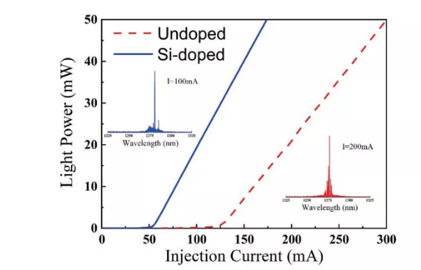
Figure 3 Comparison of power-current curves of undoped and Si-doped quantum dot lasers
2 High temperature stability
The temperature characteristics of the semiconductor laser determine the stability of the device with temperature changes and the applicable scenarios. A wider operating temperature range allows laser devices to be used in systems with harsh ambient temperatures, and at the same time enables lasers to work without cooling, reducing related temperature control parts, and greatly reducing the size and power consumption of laser modules . The high working temperature stability is the guarantee for the laser to work well, and it is also a very expected feature of quantum dot lasers.
In view of the large difference between the temperature stability of quantum dot lasers and theoretical results, some researchers have proposed the use of p-type modulation doping to improve the temperature stability of quantum dot lasers. This method has become the current method for obtaining high temperature stability quantum The most common way to point lasers.
3 high modulation rate
The 1.3 μm band is an important window of optical fiber communication, so the modulation characteristics of lasers in this band are of great significance. Directly modulated lasers transmit information by directly loading wave signals on the electrodes of the laser, which can reduce the use of external modulators and effectively save cost and space. The characterization of the modulation characteristics of the laser includes two ways of small-signal modulation and large-signal modulation response characteristics, and both indicators are very important. In optical communication systems, lasers often work under large-signal modulation. Generally, eye diagram testing is used to obtain large-signal modulation rates through a set of templates.
4 Anti-reflection characteristics
In the optical path system, the laser emitted by the laser will return to the laser cavity due to various external reflections, and this feedback light will destroy the working state of the laser. With the increase of the feedback light, the relative intensity noise (RIN) of the laser will increase, the laser linewidth will be broadened and the coherent collapse will appear, which will seriously affect the stability of the optical communication system.
Therefore, it is necessary to introduce an optical isolator in the optical system to reduce the optical feedback, but this will increase the cost and complexity of the communication system. If the laser can exhibit strong anti-reflection characteristics, the use of optical isolators can be reduced or even eliminated, which will greatly reduce the packaging cost and complexity of the system, and improve the stability of the system.
Research results in recent years have shown that quantum dot lasers show obvious advantages in anti-reflection properties.
5 Excited states and two-state lasing
InAs/GaAs quantum dot lasers, due to the discrete energy levels and finite state density of quantum dots, it is easy to observe the phenomenon of two-state lasing, that is, the ground state and the excited state are lasing at the same time. In 2003, researchers obtained two-state lasing quantum dot lasers for the first time. They believe that the behavior of two-state lasing is greatly related to the cavity length of quantum dot lasers. The two-state lasing is within the finite relaxation time of quantum dots. Produced.
Although excited-state lasing exhibits higher slope efficiency and greater output power, the higher threshold current density makes it difficult to apply in practice. For many years, researchers have been trying to suppress the emergence of excited state lasers by improving material gain, increasing device cavity length, and adopting coating methods.
However, with peoples pursuit of higher modulation rates, excited state lasers have gradually attracted the interest of researchers. Compared with the ground state laser, the excited state laser has a higher mode gain and a shorter carrier trapping time. Therefore, excited state lasing quantum dot lasers are expected to greatly improve the modulation performance of quantum dot lasers.
Si-based III-V group quantum dot laser
At present, Si-based III-V lasers are mainly prepared by bonding technology and epitaxial growth.
Bonding technology combines III-V lasers with a silicon substrate through a bonding process, which is currently a common solution in the industry. However, with the increase in demand, problems such as complex bonding technology, poor thermal conductivity of the device, and low yield have restricted its development.
Direct epitaxial growth of III-V lasers on silicon substrates is considered to be the most feasible solution for mass production of silicon light in the future. However, due to the large lattice mismatch, polarity mismatch and thermal mismatch between GaAs and Si materials, problems such as high misfit dislocation density, antiphase domains, and microcracks may occur during the epitaxial growth process. This reduces the luminous efficiency and service life of the device. Since the zero-dimensional quantum dot structure is not sensitive to dislocations, and can effectively deflect or clamp defects to prevent loop formation, position carriers, and prevent lateral diffusion or non-radiative recombination, quantum dot lasers have become popular in recent years. It has attracted great attention.
1 Direct epitaxy of bevel angle silicon substrate
Using a silicon substrate with a certain angle cut angle can effectively reduce the influence of anti-phase domains.
The researchers realized room temperature pulse lasing and room temperature continuous lasing of 1.3 μm band InAs/GaAs quantum dot lasers on a beveled silicon substrate. Later, through the study of the optical loss and reliability of lasers with different cavity lengths, it is shown that the shorter the cavity length, the faster the laser aging speed, and the more the optical loss increases. In the early stage of aging, the increase in the number of defects will increase the internal loss of the device, causing the threshold current density of the laser to increase rapidly, and the device performance is rapidly degraded. Therefore, in the actual application of the laser, the working current should be as small as possible.
The Institute of Semiconductors of the Chinese Academy of Sciences has also carried out research on Si-based and Ge-based III-V quantum dot lasers in recent years, and realized continuous lasing of 1.3 μm band InAs/GaAs quantum dot lasers on Ge/Si substrates at room temperature. In addition, many new material growth technologies have been proposed to further optimize material properties, such as the use of AlAs nucleation layers instead of GaAs nucleation layers.
2Si(001) crystal orientation direct epitaxy
Although the performance of beveled Si substrate III-V quantum dot lasers has been greatly improved, Si substrates with chamfered corners are not compatible with the complementary metal oxide semiconductor (CMOS) process of the microelectronics industry. Conducive to Si-based optoelectronic integration and mass production.
In order to achieve compatibility with the CMOS process, it is necessary to develop the technology of direct epitaxial growth of III-V quantum dot lasers on Si(001) substrates without cutting corners. The biggest challenge is how to obtain a high-quality GaAs buffer layer before growing the quantum dot structure. In recent years, researchers have done a lot of work in this area, as shown in Table 1.
It is worth noting that the threshold, power and temperature data in Table 1 that are not specially marked are the test results under the condition of continuous current injection at room temperature.
In addition to using GaP/Si (001) substrate technology, a quantum dot laser can also be prepared by growing a GaAs buffer layer after a V-shaped groove, as shown in Figure 5. Both substrates can be used to realize continuous electric lasing of micro-ring lasers.

Figure 5 Schematic diagram of the structure of a quantum dot laser prepared by a V-groove method
In addition, in 2020, the Bowers research group of UCSB in the United States used the MOCVD method to directly grow a GaAs buffer layer on a Si (001) substrate to prepare Si-based quantum dot lasers.
In 2019, the silicon-based quantum dot laser that can be continuously injected at a high temperature of 101 ℃, prepared by optimizing the material growth conditions, is the highest value of the Si-based quantum dot laser currently reported.
Prospects for the development of semiconductor quantum dot lasers
Semiconductor quantum dot lasers exhibit excellent performance in terms of threshold current density, temperature characteristics, modulation rate, and anti-reflection. 1.3 μm GaAs-based InAs quantum dot lasers exhibit a series of excellent performances such as low threshold current of 10.4 A/cm2, high operating temperature of 220 ℃, and high modulation rate of 25 Gbit/s, making quantum dot lasers suitable for high-speed optical communications and High-speed computers and other fields play an important role.
At the same time, the remarkable achievements of 1.3 m Si-based quantum dot lasers in recent years have made it close to the level of GaAs-based quantum dot lasers in some parameters, and have become an important technical means for the development of core light sources in the field of silicon-based optoelectronic integration. Promote the development of optoelectronic technology.
Currently, quantum dot lasers still have a lot of room for optimization in terms of material crystal quality, quantum dot density, quantum dot uniformity, and device design. With the development of technology, based on the advantages of quantum dot lasers with high operating temperature, high temperature stability and strong anti-reflection, quantum dot lasers working in an environment without cooling and optical isolators will significantly reduce the cost and power of the system. Consumption and volume. In the not-too-distant future, Si-based quantum dot lasers will surely drive the integration of optoelectronic technologies to produce great value in the fields of communications, medicine, and military.
Lv Zunren1,2,Zhang Zhongkai1,2,Wang Hong1,2,Ding Yunyun1,2,Yang Xiaoguang1,2,Meng Lei1,2,Chai Hongyu1,2,Yang Tao1,2
1 Key Laboratory of Semiconductor Materials Science, Institute of Semiconductors, Chinese Academy of Sciences
2 Materials and Optoelectronics Research Center, University of Chinese Academy of Sciences
Information source: OESHOW
This information is from the Internet for academic exchanges. If there is any infringement, please contact us and delete it immediately