01
The background of parallel laser micro-nano processing technology
Lithography is one of the most commonly used techniques in semiconductor manufacturing, and it is the basis of modern optoelectronic device manufacturing. However, deep ultraviolet and extreme ultraviolet lithography systems and their corresponding optical masks are all based on low-speed and high-cost electron beam lithography (EBL) or focused ion beam etching (FIB) technology, resulting in relatively expensive prices. Therefore, the maskless high-speed fabrication method is the preferred method for the fabrication of micro-nano structures.
Among these maskless methods, direct laser writing (DLW) is an important and widely used micro-processing technology that can provide the lowest price and relatively high throughput. However, there are two main challenges in practical applications: one is that the resolution is not high enough compared with FIB and EBL; the other is that the direct laser writer generates patterns point by point, so throughput is a big challenge.
For the above two challenges:
In terms of resolution, first, it can be improved by near-field technologies such as atomic force microscopy (AFM) or scanning near-field microscopy (SNOM), second, it can be improved by using short-wavelength light sources, and third, super-resolution can be achieved through nonlinear absorption. Imaging or manufacturing;
In terms of manufacturing speed, in addition to engineering methods, with the development of laser technology, parallel laser processing methods including self-assembled microsphere laser processing, laser interference lithography, and multifocal array laser direct writing are mainly proposed to increase manufacturing speed.
Parallel laser processing technology can extend two-dimensional processing technology to three-dimensional processing, providing a new direction for the development of micro-nano processing technology in the future; at the same time, it can be widely used in surface treatment and functional device manufacturing in the fields of sensing, solar cells and metamaterials It is of great significance to the development and research of biomedical device manufacturing, optical communication, sensing, and spectroscopy.
02
Implementation of parallel laser micro-nano processing technology
The realization of parallel laser micro-nano processing technology can be mainly divided into: contact type and non-contact type.
2.1 Contact parallel laser processing technology
Contact parallel laser processing technology refers to the use of microsphere particles for laser patterning.
Mechanism of laser nanofabrication of microspheres
Microsphere laser nanofabrication technology originally originated from research in the field of laser cleaning. Research has found that after the small spherical particles on the substrate are irradiated by the pulsed laser, the center of the spherical particles on the substrate can produce micro/nanopores of subwavelength size. For metal particles, this is caused by the enhancement of the strong electromagnetic field generated by the LSPR between the particles and the substrate; for medium particles, since most of them are transparent, the transparent particles can be regarded as microsphere lenses, and the incident light The electromagnetic field enhancement caused by focusing on the bottom surface of the microspherical lens. This process can achieve a 60-fold increase in the intensity of the incident light. By designing the diameter, refractive index, environment, and incident laser intensity of the microspheres, it is possible to ablate micro/nanopores with sub-wavelength dimensions on the substrate.
Realization of laser nano-processing of microspheres
Regarding the microsphere laser nanomachining technology, according to the different ways of manipulating microsphere particles, it can be divided into two categories:
One is to use optical tweezers technology to manipulate microsphere particles to create arbitrary patterns;
The second is to use self-assembly technology to manufacture microsphere array masks.
This parallel laser processing based on microspheres is a relatively economical method in nanomanufacturing.
Use optical tweezers technology to manipulate microspheres to create arbitrary patterns
For optical tweezers technology to manipulate microspheres to create arbitrary patterns, this process can be divided into two steps:
First of all, due to the small size and light weight of the microspheres, the laser is used to confine the microspheres in the potential well and distribute them parallel to the sample surface. During this process, the laser will not ablate the substrate;
Then, another pulsed laser is used for ablation to form a pattern on the substrate.
Among them, the function of the microsphere is similar to the AFM or SNOM tip in the lithography system. The pattern made in this way has complete freedom, but the processing speed is still slow.
In order to avoid the impact of the slow manufacturing speed caused by the single trapping of particles, multiple potential wells can be generated through a specially designed light distribution to achieve simultaneous control of multiple microspheres. Or by moving the sample stage to create any periodic pattern, and then use the parallel laser to ablate the sample.
Self-assembled microsphere array
The specific method of manufacturing microsphere arrays using self-assembly technology is as follows:
The colloidal particle solution is first applied to the surface of the substrate and dried in the air to form a tightly arranged array of microspheres. The effect is related to the wettability of the substrate and the concentration of the "microsphere solution".
Then a pulsed laser beam is applied to directly ablate the surface of the sample through the microspheres.
Different from using optical tweezers technology to manipulate microspheres, through self-assembly technology, the microsphere array is fixed on the sample surface, and relative movement cannot occur on the sample surface. Therefore, the formation of the sample surface pattern mainly depends on the symmetry of the microspheres. Since the self-assembled microsphere array will produce many focal points, when the laser illuminates the sample at a certain incident angle, the light can be focused on different positions on the sample surface. By changing the incident angle of the laser and scanning the sample with the focus, large-area and periodic patterns can be made directly on the target surface flexibly without pattern transfer.
However, the limitation of self-assembly technology is that the microspheres on the surface of the sample must be washed off after laser processing, and because the microspheres are randomly distributed during the self-assembly process, defects in mass production cannot be avoided, and multiple exposures cannot be performed.的Alignment.

Figure 1. Schematic diagram of the contact type parallel laser processing technology and the electron microscope image of the nano-patterns processed by this technology.
2.2 Non-contact parallel laser processing technology
There are two ways of non-contact parallel laser processing technology: one is laser interference lithography; the other is far-field multifocal array nanolithography.
Laser interference lithography
Laser interference lithography (LIL) technology is one of the most classic methods of maskless exposure, which mainly utilizes the coherence of lasers. Since LIL technology is usually used to expose photosensitive materials, subsequent processes such as reactive ion etching (RIE) and lift-off processes are required to transfer the pattern from the photosensitive layer to the target surface. However, with the commercialization of high pulse energy lasers, LIL is no longer limited to photosensitive materials, and can directly ablate other materials, such as silicon, gallium, and zinc sulfide materials. This extended method is called laser interference ablation. Law (LIA). Generally speaking, dual-beam interference technology is mainly used to manufacture one-dimensional line arrays or two-dimensional hole/disk arrays. Therefore, the use of LIL to manufacture large-scale line or dot arrays has the advantages of low cost and high efficiency. However, its disadvantage is that the pattern is single, limited to gratings or dots, and only two-dimensional. If it is combined with wet etching technology, the made two-dimensional pattern can be expanded in another dimension to form a three-dimensional structure; if you want to make any form of pattern or structure, you need to further expand the number of interference beams , That is, the use of multi-beam interference technology can achieve 3-dimensional periodic structure manufacturing.
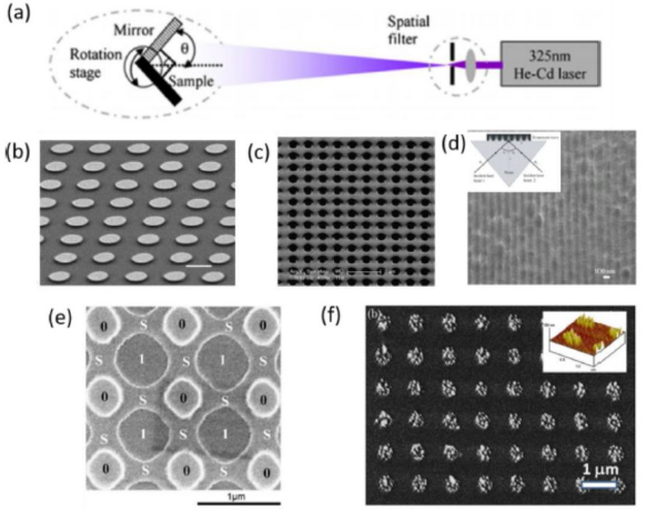
Figure 2. The device diagram of laser interference lithography and the nano-patterns produced by the technology.
Far-field multifocal array nano pattern
In traditional laser processing, a parallel laser beam passes through a lens and is focused into a single point. The focal point can be used for direct laser writing. The focus array means that there are a large number of "pens" that can be used to write patterns in parallel. If the number in the focus array is N, the pattern formation speed can be increased by N times. Therefore, the use of multi-focus arrays to write nano patterns can be revolutionary To improve the manufacturing speed of traditional DLW.
For the generation of multifocal arrays, there are several different ways: one is through microlens arrays (MLA); the other is through spatial light modulator (SLM), digital mirror Diffractive optical elements (DOE) including equipment and Daman grating to generate a multi-focus array. Finally used for parallel laser processing.
Microlens array method
MLA is a unique optical component consisting of thousands of lenses with a diameter of micrometers. MLA is usually manufactured through a semiconductor manufacturing process. For devices that use MLA to achieve parallel laser processing, a microlens array direct laser writing (MLA-DLW) system is typical. In this system, the shutter is used to control the exposure time, and the beam expander is used to adjust the laser beam to match the size of the MLA, and the expanded beam illuminates the entire MLA. Place the sample on the seven-axis nano-stage to precisely control the gap between the sample and the MLA. Through the computer numerical control (CNC) program to control the shutter switching and the movement of the nano translation stage, 2D (or even 3D) patterns can be made. The resolution of the mode is limited by the length and NA of the MLA. Through MLA-DLW technology, all periodic microstructures can be manufactured at low cost, high speed, and high uniformity.
However, the resolution of the MLA-DLW system is also limited by the optical diffraction limit. The typical resolution of MLA-DLW technology is about 1μm. If the laser light source is changed to short-wavelength ultraviolet light, the optical components of the entire system need to be replaced with expensive components suitable for ultraviolet light, which increases the cost. Therefore, if the MLA, relay lens and high NA oil immersion objective lens are combined together, the focal point generated by the MLA can be projected onto the photoresist to manufacture a dot array with a feature size of about 250 nm. MLA performs vector scanning and can realize a 3D sub-wavelength periodic spring structure array.
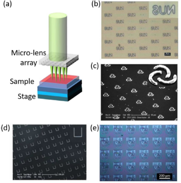
Figure 3. Schematic diagram of the MLA-DLW system and nano patterns processed by this technology.
Multi-focus array laser pattern based on diffractive optical element
Using a spatial light modulator (SLM), light can be modulated in different modes by holographic technology. The process is:
First, irradiate the laser on the SLM to change the phase distribution of the light;
Then, a 4f imaging system is used to project the beam from the SLM to the objective lens. Add a filter to the Fourier plane of the 4f system to select the first diffraction order.
Finally, the objective lens is used to perform Fourier transform on the laser with phase distribution, and lithography is performed on the photoresist.
In theory, any pattern can be made with this method through proper design.
In addition, a Daman grating can be used instead of STM to generate multiple beams along different directions. These diffracted multiple beams can be Fourier transformed to multiple focal points through the objective lens, and then the 4f system is used to project the distribution of the vector light field onto the objective lens. Filter high-order diffraction orders. All these methods can realize non-contact parallel laser processing.
03
Application case study
Based on these parallel laser processing technologies, various functional devices can be flexibly processed and manufactured. These functional devices can be divided into three types according to the application: sensing, anti-reflection/black surface and metamaterials.
3.1 Sensing
There are two ways to apply the above functional devices in the sensing field: one is SERS-based Raman spectroscopy detection, and the other is surface plasmon resonance (SPR) sensing.
Raman spectroscopy can clarify the vibration and rotation information of molecules, but because the Raman signal is very weak, there are strict requirements on the detection system. The intensity of the Raman signal is proportional to the fourth power of the electric field intensity. However, the stronger laser intensity will damage the sample, so metal nanostructures can be used cleverly to achieve local electromagnetic field enhancement to achieve Raman signal amplification. Compared with photolithography technology, LIL technology has strong flexibility in SERS substrate manufacturing. For example, in orderly SERS substrate manufacturing, LIL technology can adjust the period of the structure to match the Raman excitation line, which is compatible with the Raman characterization system. The laser wavelength achieves resonance.
Surface Plasmon Resonance (SPR) sensing is based on the resonance frequency shift or intensity modulation caused by changes in the environmental refractive index. Since the wave vector of SPP is larger than the wave vector in mid-air, the excitation of SPP needs to meet a higher wave vector. The traditional way of exciting SPP is grating coupling or large-angle incidence based on prism. Both methods require off-axis illumination. The nano-patterned lattice manufactured by LIL technology or other parallel laser processing technology can provide additional wave vectors for incident light, so off-axis illumination is no longer required, so that the SPR sensor can be compatible with the spectrum detection device under normal illumination. In addition, compared with random nanodots produced by chemical methods or thermal annealing, the rapid production of ordered dot arrays by LIL or other parallel laser processing techniques can provide higher sensitivity for SPR refractive index sensing.
3.2 Anti-reflective surface
Anti-reflective coating (ARC) has aroused great interest in various fields. For example, photovoltaic devices, light-emitting diodes (LEDs), light sensors and optical components/windows all require low-reflectivity surface structures. In order to achieve this goal, the size of the structure needs to be smaller than the wavelength to reduce the reflection effect at the interface. Common structures include gratings, pyramids, porous structures, etc., although these surface structures can also be manufactured by other nanomanufacturing methods, such as EBL. But compared with EBL, LIL has higher speed and lower cost, especially in large-area manufacturing of these micro/nano structures has unique advantages. In addition, if you want to further reduce the reflectivity of the surface structure, you can also apply a hybrid method. For example, combining the LIL technology and the film deposition method, supplemented by wet etching, can achieve a maximum reflectivity of 1.0% and an average reflectivity of 0.8%.
3.3 Metamaterials
Metamaterials are periodic sub-wavelength structures that can manipulate electromagnetic waves. The currently widely used terahertz (THz) metamaterials have feature sizes on the order of micrometers, which can be easily achieved by direct laser writing or photolithography, but these methods are relatively It is slow, so the MLA-DLW system in parallel laser micro-nano processing technology has become one of the best solutions to this problem. Take the classic split-ring resonator (SRR) structure as an example. Using the MLA-DLW system, only a simple loop path is needed to expose the periodic SRR structure array in a short time. After patterning, film deposition and lift-off processes are used to transfer the structure from the photoresist. Therefore, the MLA-DLW system greatly improves the processing speed of terahertz metamaterials and expands the processing scale. In turn, the development of metamaterials has further promoted the advancement of MLA-DLW technology. For example, the successful production of metamaterials on flexible substrates has further developed the new application of MLA-DLW technology in flexible electronic products.
04
Analysis of the advantages and disadvantages of different processing technologies
Processing methods
Advantage
Disadvantage
Contact
Nanofabrication of microspheres
Due to the near-field effect, optical super-resolution can be achieved
Optical tweezers technology is too slow to manipulate microsphere particles
Compared with the traditional near-field direct writing method based on AFM / SNOM "pen point", it can not only significantly increase the manufacturing speed, but also avoid the wear of the "pen point"
The distribution process of the microspheres in the self-assembly process is not controlled, and mass production cannot be carried out, resulting in the technology being limited to scientific research rather than industrial production
Contactless
LIL technology
principle Simple, mature design, can make patterns on a large area with high resolution and low cost, widely used in scientific research and industrial production
Can only make periodic patterns
MLA-DLW
Compared with the traditional DLW system, it can manufacture arbitrary periodic structures at a higher speed, realizing low cost and high yield
The patterns produced must be periodic, and arbitrary patterns cannot be processed
DOE-based multi-array nanofabrication
Flexible design, any pattern can be obtained
The laser processing system is complicated and limited to scientific research
Parallel laser micro-nano processing technology is divided into two categories: contact and non-contact.
The contact type mainly refers to the use of microsphere particles for laser patterning.
Its advantages are: firstly, the contact mode can achieve optical super-resolution due to the near-field effect; secondly, compared with the traditional near-field direct writing method based on the AFM/SNOM "pen tip", it can not only significantly increase the manufacturing speed, but also Avoid the wear of the "pen nib".
Its disadvantages are: first, the distribution process of microspheres is not controlled in most cases, so there are still many challenges in large-scale production; second, defects cannot be avoided in large-area manufacturing, resulting in this technology being only used for scientific research rather than industrial production .
In contrast, non-contact types mainly include LIL, MLA-DLW system, and DOE-based multi-focus array laser patterning technology. The advantages and disadvantages are described separately here.
The advantages of LIL technology are: First, it can make patterns on a large area with high resolution and low cost, and because of its simple principle and mature design, it can be widely used in scientific research and industrial production;
The disadvantage is that only periodic patterns can be made.
The advantage of the MLA-DLW system is: Compared with the traditional DLW system, it can manufacture arbitrary periodic structures at a higher speed, achieving low cost and high output;
The disadvantage is that only periodic patterns can be produced, and arbitrary patterns cannot be processed.
The advantage of DOE-based multi-focus array laser patterning technology is that it can design any pattern;
The disadvantage is: the system is complex