LEGO bricks are perhaps the most fascinating childhood of any child, and the best educational toy that can use imagination and creativity. Although the simplest materials and the simplest combination are used, starting from these simple building blocks and exerting creativity, you can build a variety of amazing works. For physical and materials scientists, two-dimensional materials in nature are excellent Lego blocks; stacking different two-dimensional materials through weak van der Waals forces (weak interactions between neutral molecules or atoms) The "Van Derwa heterojunction" formed together is the most interesting Lego work in their eyes, and it is also a "new continent" that brings them endless research fun. This article will take the 13 Nature / Science published this year as an example to introduce the new direction of the two-dimensional materials research field of new van der Waals heterojunctions.

1.Nature: Van der Waals integration strategy for multi-dimensional materials

Material integration strategies often involve strong chemical bonds (such as epitaxial growth) and are usually limited to materials with a high degree of structural matching and process compatibility. Through weak Van der Waals interactions, the prefabricated building units are physically assembled together, which can achieve integration without chemical bonds, which can get rid of the constraints of lattice and processing technology (such as two-dimensional Van der Waals heterostructure). Recently, UCLA Duan Fengfeng and Huang Yu reviewed the development, challenges, and opportunities of this emerging method, and summarized it as the flexible integration of multiple material systems with multiple dimensions (beyond two dimensions), and discussed their beyond The potential of man-made heterostructures or superlattices in the range of available materials.
Literature link:
https://www.nature.com/articles/s41586-019-1013-x
2.Nature: Evidence of Moore excitons in van der Waals heterojunction
 University of Texas at Austin Li Xiaoqing / Argon National Laboratory Wu Fengcheng reports positive or negative circular polarization in a heterobilayer / tungsten diselenium (MoSe2 / WSe2) heterolayer with a small twist angle Observation of Multiple Interlayer Exciton Resonances Emitted Researchers attribute these resonances to the ground state of the exciton and the excited state restricted by the Moire potential. This explanation is supported by recombination kinetics and the dependence of these interlayer exciton resonances on torsion angle and temperature. These results indicate the feasibility of designing artificial exciton crystals using van der Waals heterostructures for nanophotonics and quantum information applications.
Literature link:
ttps://www.nature.com/articles/s41586-019-0975-z
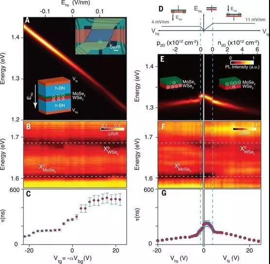
3. Nature: Interlayer valley exciton that captures Moire potential in heterogeneous layers of MoSe2 / WSe2

Xu Xiaodong from the University of Washington / Wang Yao from the University of Hong Kong reported experimental evidence of interlayer valley exciton trapping of Moire potential in the heterolayer of molybdenum diselenide (MoSe2) / tungsten diselenide (WSe2). In the twisted MoSe2 / WSe2 double-layer two-dimensional heterojunction, the researchers successfully captured the interlayer valley exciton of the Moire potential. At low temperatures, researchers have observed that the photoluminescence energy is close to the free-layer exciton energy, but the line width is more than a hundred times narrower (about 100 meV). For a given twist angle, the emitter exhibits strong circular polarization with the same helicity, which indicates that the trapping potential maintains triple rotational symmetry. Combining the characteristic dependence on power and excitation energy, the researchers believe that the observed effect results from the interlayer exciton being trapped in a smooth Moore potential. These results indicate that the origin of the observed effect is that interlayer excitons are trapped in a smooth Moore potential with inherited valley contrast physics. This work provides an opportunity to control 2D Moire optics by changing the twist angle.
Literature link:
https://www.nature.com/articles/s41586-019-0957-1#auth-8
4.Nature: Moire exciton found in WSe2 / WS2 heterojunction

Moore superlattices can generate new quantum phenomena in two-dimensional heterojunctions, where interactions between thin layers of atoms can change the electronic band structure of the superlattice. For example, tiny Dirac points, tunable Mott insulator states, and Huffstatt butterfly modes appear in different types of graphene / boron nitride Mohr superlattices, but related insulation and superconductivity Properties have been reported in distorted double graphene moire superlattices. In addition to the obvious effects on single particles, Mohr superlattices have been predicted to be host excited states, such as Mohr exciton bands. Here, Feng Wang‘s team at the University of California, Berkeley, found the Mohr superlattice exciton state in the WSe2 / WS2 heterostructure. These Moire exciton states appear as multiple peaks in the absorption spectrum, around the initial WSe2 A exciton resonance, and they exhibit A in a WSe2 monolayer and a WSe2 / WS2 heterostructure with a large twist angle Excitons have different gate dependencies. These phenomena can be described by a theoretical model in which the periodic Moire potential is much stronger than the exciton kinetic energy, and multiple planar exciton microbands are generated. Moore exciton bands provide an attractive platform from which to explore and control the excited states of matter, such as topological excitons and related exciton Hubbard models in transition metal disulfides.
Literature link:
https://www.nature.com/articles/s41586-019-0976-y
5.Nature: Resonant hybrid exciton in the van der Waals heterojunction Mohr superlattice
 A two-dimensional material with atomic layer thickness can be assembled by vertical stacking under the action of weak Van der Waals forces, thereby achieving coupling between two crystals that are not coherent and can rotate arbitrarily with each other. It is for this reason that the atomic sites in this type of structure produce an important periodicity-the Mohr superlattice. In the graphene / hexagonal BN heterojunction, the presence of Mohr superlattice allowed researchers to observe the electron microstrip, while in the twisted graphene double-layer structure, its effect was strengthened due to interlayer resonance conditions, leading to Superconductor-insulator transition at magic angle. The Alexander I. Tartakovskii team at the University of Sheffield, UK, and the Vladimir I. Fal′ko team at the University of Manchester, using non-coherent single-layer WSe2 / WS2 semiconductor heterojunctions, proved that exciton bands can be hybridized, which in turn led to Moore Ultra Lattice effect resonance strengthens. The authors chose the WSe2 / WS2 system because the near degeneracy of the conduction band edges can promote intra- and inter-layer exciton hybridization. In the study, hybridization is shown by the phenomenon that the significant exciton energy shift is a periodic function of the interlayer rotation angle, and the periodicity of the exciton energy shift is because the hybrid exciton is generated by the holes in MoSe2, and MoSe2 interacts with the superposition of torsion-dependent electronic states in adjacent monolayers. For a nearly uniform coherent heterojunction of a single-layer structure, the resonant mixing of electronic states makes the geometric moire fringes of the heterojunction have a significant effect on the dispersion and spectrum of the hybrid exciton. In the field of semiconductor devices based on van der Waals heterojunction, this research enriches the strategy of band engineering.
Literature link:
https://www.nature.com/articles/s41586-019-0986-9
6.Nature: Van der Waals interaction between 3D metals and 2D semiconductors
 With the reduction of the size of the semiconductor channel in the field effect transistor, the contact resistance of the metal-semiconductor interface at the source and the drain increases, which affects the performance of the device. Two-dimensional (2D) transition metal disulfides, such as molybdenum disulfide (MoS2), have proven to be excellent semiconductors for ultra-thin field effect transistors. However, an abnormally high contact resistance was found at the interface between the metal and the two-dimensional transition metal disulfide. Recent studies have shown that van der Waals interactions between graphene and transition metal disulfides and metals and transition metal disulfides have achieved good contact properties. However, van der Waals interactions between three-dimensional metals and single-layer two-dimensional transition metal disulfides have not been confirmed. In view of this, Manish Chhowalla et al. Deeply studied the van der Waals interaction between the 10nm-thick indium metal coated with gold nanoelectrodes and the monolayer MoS2. Scanning transmission electron microscopy imaging confirmed the van der Waals interaction between metal indium and molybdenum disulfide. The contact resistance of the single-layer MoS2 indium / gold electrode is 3000 ± 300 ohms, and the multilayer MoS2 is 800 ± 200 ohms. These values are one of the lowest values observed at the interface between a three-dimensional metal electrode and molybdenum disulfide, and enable the mobility of high-performance field-effect transistors to reach 167 ± 20 cm 2 per volt per second.
Literature link:
https://www.nature.com/articles/s41586-019-1052-3
7.Nature: Chiral twisted van der Waals nanowires
 Peter Sutter and Eli Sutter of the University of Nebraska demonstrated a class of materials-layered crystal van der Waals nanowires, in which tunable interlayer distortions evolve naturally during synthesis. In gas-liquid-solid growth, GeS nanowires (anisotropic layered semiconductors) are layered and crystallized along the axis, and have a clear tendency to form axial spiral dislocations. Nano-resolution electron diffraction shows that due to the stress field of axial dislocations, Eshelby distortion is caused by the torque on the end of the cylindrical solid, which in turn causes a chiral structure in the van der Waals nanowires. Studies have shown that the in-plane GeS crystal axis gradually rotates along the line, and the spiral adjacent GeS layers naturally form Moire patterns due to interlayer distortion. The axial rotation and twist can be adjusted by changing the thickness of the nanowires. This study demonstrates that the moiré pattern between the boundary layers is realized along a spiral path on the nanowire instead of a flat interface, making scalable manufacturing of Van der Waals structures with defined twist angles an important step forward.
Literature link:
https://www.nature.com/articles/s41586-019-1147-x
8.Nature: Helix twisted van der Waals structure
 A common fabrication strategy for twisted van der Waals structures is the transfer-stack process. One disadvantage of this method is that it cannot be used for materials with relatively strong interlayer forces. As a result, scientists began to explore simple, bottom-up methods to make more twisted Van der Waals structures. In view of this, Jie Yao‘s research team at the University of California, Berkeley, based on Eshelby distortion, obtained a spirally twisted van der Waals structure. Studies have shown that Eshelby distortions associated with spiral dislocations (chiral topological defects) can drive the formation of Van der Waals structures from nanoscale to mesoscale, and can also customize the twisted topology by controlling the radial size of the structure. During the synthesis process, the research team first introduced axial helical dislocations into GeS nanowires grown along the stacking direction to produce van der Waals nanostructures with continuous twists, where the total twist rate was defined by the radius of the nanowires. Because the total twist rate is fixed by the substrate, the twisted nanowires attached to the substrate grow further radially, which results in an increase in elastic energy. By regulating the fixed twist rate in a series of discrete jumps, the stored elastic energy can be reduced, resulting in a mesoscopic scale twist structure, which is composed of spiral assembled nanoplates.
Literature link:
https://www.nature.com/articles/s41586-019-1308-y
9.Nature: Regulation of superconducting properties of three-layer graphene / hBN van der Waals heterojunction
 The three-layer graphene (ABC-TLG) / hBN heterojunction provides an ideal platform for the systematic study of the triangular Hubbard model: theoretical calculations show that the triangular superlattice of the heterojunction system shows a nearly flat independent For microstrip, the bandwidth of the microstrip can be adjusted by changing the vertical electric field. In contrast, magic angle twisted double-layer graphene exhibits two flat microstrips and always intersects in a single-particle strip structure. In view of this, teams such as Feng Wang of the University of California, Berkeley, Yuanbo Zhang of Fudan University, and David Goldhaber-Gordon of Stanford University reported that in the 1 / 4-filled Mott state, three-layer graphene (ABC-TLG) / hBN heterojunction in Characteristics of regulatory changes in the transduction structure. 1) The researchers observed two distinct superconducting domes when electron and hole doping were performed relative to the 1/4 filled Motte state. 2) The authors also found that by controlling the vertical electric field, transitions between superconducting, insulating, and metallic states in the ABC-TLG / hBN heterostructure are easy to occur.
Literature link:
https://www.nature.com/articles/s41586-019-1393-y
10.Nature: Research on Visual Characterization of Electrostatic Gating Effect in 2D Material Van der Waals Heterojunction
 In field-effect transistors, direct observation of electronic states (such as local potential changes, Fermi levels, band structures, etc.) can deepen our in-depth understanding of physics, thereby helping us to continuously improve the function of the device. In view of this, teams such as Xiaodong Xu, David H. Cobden of the University of Washington, and Neil R. Wilson of the University of Warwick reported a micro-scale angle-resolved photoelectron spectroscopy that can realize the electronic state of two-dimensional van der Waals heterojunction devices. Monitoring research. It is worth mentioning that the detection can be performed on a single device, so that the relationship between the electronic and optical characteristics of the gate control can be studied in depth and accurately. The authors found that when a gate voltage is applied in a double-ended graphene device, the Fermi level shifts, crosses the Dirac point, and the dispersion hardly changes. In two-dimensional semiconductor devices, the edges of the conduction band are continuously accumulating electrons, and the energy and momentum of the edges are continuously gathered. In single-layer WSe2, as the electrostatic doping increases, the band gap drops to several hundred meV, which is close to the exciton energy.
Literature link:
https://www.nature.com/articles/s41586-019-1402-1
11.Nature: Interlayer exciton laser with extended spatial coherence in the nucleus
 Two-dimensional semiconductors have become a new type of nanophotonic materials due to their strong exciton-photon interactions and engineering and integration flexibility. Utilizing these characteristics, Hui Deng et al. Of the University of Michigan designed an efficient laser medium based on Dipoar interlayer exciton. The medium has a rotating heterogeneous atomic thin structure. Measurement of lasing from a transition metal hydrogen dihalide heterobilayer integrated in a silicon nitride gate resonator. A sharp increase in the spatial coherence of the emission was observed across the emission threshold. This work establishes interlayer excitons in a two-dimensional heterostructure as coherent media compatible with silicon. These interlayer excitons have electrically tunable optical-matter interaction intensity and long-range dipole interactions, so they are expected to be applied to low-power, ultrafast lasers and modulators, and rich multibody quantum phenomena.
Literature link:
https://www.nature.com/articles/s41586-019-1779-x
12.Science: Two-dimensional heterojunction extends exciton life
Excitons (combination pairs of electrons and holes in solids) can in principle be used as information carriers. However, since electrons and holes tend to recombine quickly, their lifetimes are limited. One way to extend life is to physically separate electrons and holes, such as by placing them in different layers of van der Waals‘ heterostructure. For this reason, Harvard‘s Philip Kim team used this strategy to form long-lived interlayer excitons in a van der Waals heterostructure consisting of a single layer of molybdenum diselenide (MoSe2) and a single layer of tungsten diselenide (WSe2). By electrically controlling the layers in the heterostructure, the researchers further increased the exciton lifetime and formed and manipulated the charged exciton.
Literature link:
https://science.sciencemag.org/content/366/6467/870
13.Science: Van der Waals stack-dependent interlayer magnetism
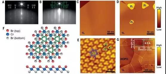
Through extensive research on two-dimensional magnetic materials, scientists have discovered many related van der Waals materials, such as chromium triiodide (CrI3) and chromium tribromide (CrBr3). Although they have similar properties in theory, in the double-layer form, the former is antiferromagnetic, while the latter seems to be ferromagnetic. The magnetic coupling characteristics between two-dimensional layered magnetic materials may bring new ideas for the development of new magnetic devices. Considering the weak atomic interlayer van der Waals forces between two-dimensional layered magnetic materials, this makes it possible to artificially construct interlayer van der Waals stacks. In view of this, Fudan University‘s Gao Chunlei‘s team and Wu Shiwei‘s team collaborated to study how the magnetic state of the double-layer CrBr3 depends on the type of single-layer stack. The research team used a self-developed spin-polarized scanning tunneling microscope and other methods to find that when two monomolecular layers are oriented in the same direction, an antiferromagnetic state is formed, and the opposite orientation results in ferromagnetism.
Literature link:
https://science.sciencemag.org/content/366/6468/983
This article is contributed by eric.
Source-WeChat public: material source