
Research Background
Due to the weak interaction between neutrons and most substances, direct detection of neutrons faces great challenges. Neutron detectors use the properties of certain nuclides. These nuclides will decay into high-energy charged fragments after capturing neutrons. In fact, only 3He, 10B, and 6Li combine high-neutron capture crossovers and detectable decay. Products, and these isotopes are currently used in various detector structures.
Efficient neutron detectors are serious in many fields such as national security, medicine, astronomy, and so on. There are two main types of neutron detectors currently in use: gas detectors and scintillator detectors. Detectors, semiconductor neutron detectors are smaller and have advantages in some aspects, so they have become the focus of research for some scientists. Semiconductor neutron detectors are divided into two categories: indirect and direct conversion detectors. The thermal neutron detection efficiency of indirect conversion semiconductors is up to about 40%, while direct conversion semiconductors use a single material for neutron capture and scattering collection to achieve Simple detector geometry with inherent thermal neutron detection efficiency approaching 100%. However, since the neutron flux may be very low and the number of excitations generated is very small, the semiconductor must be very pure and the carrier capture rate must be low. Therefore, the semiconductor materials that can be used for neutron detectors are not easy to find. Among them, 6Li is considered to be an ideal predetermined material because of its excellent neutron absorption capacity. However, Li will break up when it encounters water. Semiconductor neutron detection also needs to solve the problems of how to integrate lithium into the semiconductor and convert it stably.
Achievements
The material has a good thermal neutron capture cross section, a suitable band gap (2.06 eV), and an energy band structure capable of effectively transmitting bandwidth. Using alpha particles from the 241Am source as a substitute for the neutron capture reaction, the two-dimensional LiInP2Se6 detector can resolve the full energy peak with an energy resolution of 13.9%, while using the appropriate 6Li (95%) 6LiInP2Se6 full peak resolution detection This device can directly detect the decelerated Pu-Be neutron source. In various fields, small neutron detectors have a lot of application space. The research results will stimulate scientists‘ interest in semiconductor neutron detectors, so that semiconductor-based neutron detectors will replace 3He counters. A neutron gas detector). The topic "Direct Thermal Neutron Detection by 2D Semiconductor 6LiInP2Se6" was published in the top journal Nature.
Graphic guide

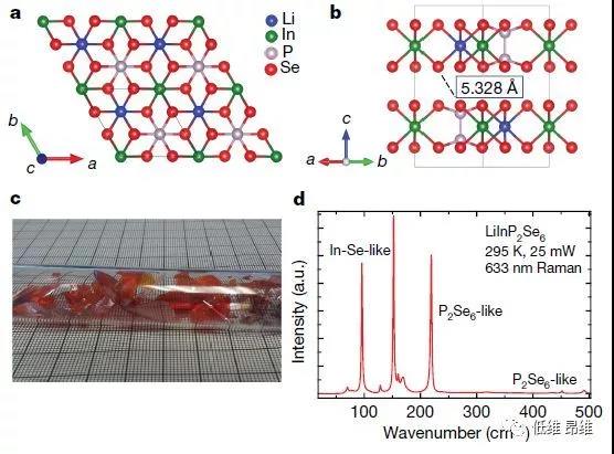
Figure 1. Structural characteristics of LiInP2Se6.
(A, b) Crystal structure of LiInP2Se6. LiInP2Se6 is a two-dimensional layered semiconductor. Each layer is combined with Van der Waals force. Each individual layer has a crystal structure of CdI2. Among them, Li, In, and P2 occupy the third of the octahedral Cd position in an ordered manner. One, Se occupies the I position, and these layers are stacked in order of ABAB to align the InSe6 polyhedron, while the LiSe6 and P2Se6 polyhedrons alternate along the c-axis.
(C) LiInP2Se6 lamellar crystals grown by CVT on the raw material side of the reaction vessel.
(D) The Raman spectrum of LiInP2Se6 collected at room temperature shows several easily resolved peaks under the excitation of 633 nm, which is consistent with the characteristic vibration modes associated with the In-Se bond and the P2Se6 unit.

Figure 2. Band structure and optical properties of LiInP2Se6 single crystal.
(A, b) Electron band structure and density of states. The calculation of the density functional theory of the electronic energy band structure is performed using PBE + vdW functional. It shows that LiInP2Se6 is an indirect band gap semiconductor. The band gap is 0.94 eV. The conduction band consists of the In s and Sep hybrid states associated with the empty In 5s lone pair, while the valence band consists of the Sep states. The conduction band has a high curvature, corresponding to low effective electron masses (me *) in the in-plane and out-of-plane directions of 0.16 me and 0.30 me, respectively. The maximum value of the valence band is along the out-of-plane in the reciprocal space (K to H) Direction, and the valence band in that direction is very flat, so the effective mass of holes in the out-of-plane direction will be large. Considering that the planar properties of the material make the device work in an out-of-plane direction, the electron mobility in LiInP2Se6 is expected to be very superior.
(C) The UV-Vis-NIR transmission spectrum of LiInP2Se6 is used to measure the band gap, which is 2.06 eV.
(D) PL spectra and PL emission images of LiInP2Se6 at 12.5 K and 2 mW. The surface of the grown single crystal excites red-orange emission light, and two broad emission bands can be observed, with the maximum peaks around 1.73 eV and 2.05 eV. The PL test related to excitation intensity and temperature showed that the peak at 1.73 eV was a donor-acceptor pair recombination, and the peak at 2.05 eV was a free-binding transition. Despite these defect-related peaks, a strong PL signal from this indirect band gap material indicates good optical quality.

Figure 3. Electrical characteristics and pulse height spectrum of LiInP2Se6 device irradiated with alpha particles and gamma rays.
(A) For LiInP2Se6 (~ 0.3 mm thickness) grown by CVT with gold electrode, dark current and photocurrent (absolute value) and voltage (-100 V to 100) under ambient light (~ 0.2 mW cm-2) V) relationship. The original LiInP2Se6 device exhibited very low dark current, about picoamperes, corresponding to a high resistivity of about 1013 Ω cm. When exposed to ambient light (~ 0.2 mW cm-2), the photo-generated charge carriers in the LiInP2Se6 detector increase the current by three to four orders of magnitude. This is an excellent optical response, indicating that LiInP2Se6 has good Charge transfer characteristics.
(B) Pulse height spectra of LiInP2Se6 devices (thickness of about 120 μm) irradiated with 5.486 MeV 241Am α particles at different voltages, used for electron collection, each collection for 60 s. As a higher charge collection efficiency (CCE) can be obtained under a higher applied electric field, as the voltage increases, the peaks generated by the alpha particle interaction move to a higher number of channels. The energy resolution of the full energy peak of the LiInP2Se6 detector at 700 V is 13.9%, which indicates that LiInP2Se6 can accurately analyze the charged particles generated by neutron interactions. For a constant voltage applied to various samples, the CCE is higher for thinner samples due to the larger external electric field. These results finally prove that LiInP2Se6 device can achieve high-resolution spectral response to 241Am α particles.
(C) Pulse height spectrum of LiInP2Se6 detector (approximately 0.5 mm thickness) under 700 V bias when irradiated with γ-rays from 241Am and 57Co and passive. The counts for 57Co gamma rays and natural background are negligible, and the spectra are collected 200 s at a time. An ideal neutron detector should be insensitive to gamma rays to ensure that no false neutron counts are caused by incident gamma radiation. Despite the high flux, the environmental background and pulse height spectrum under direct gamma radiation are basically the same. It shows that the material‘s sensitivity to gamma rays is negligible.
(D) Pulse height spectrum at 700 V under the same conditions as in b. In a-d, the contact area on the crystal is 3 × 3 mm2, and the forming time in b-d is 1 μs. When a large voltage is applied, a diode-like current-voltage curve is observed. At 1000 V, the low dark current is maintained at 2 nA, which is sufficient for effective detection of alpha particles and neutrons. This electrical behavior may be in Caused by blocking / injection current from the electrodes under a large electric field of up to several tens of kilovolts / cm.

Figure 4. Thermal neutron spectrum of a 6LiInP2Se6 device. At room temperature, the thermal neutron response of a 95% 6Li-rich detector was tested using a slow and very weak Pu-Be source that produced approximately 75 neutrons per square centimeter per second.
(A) Exposure to an unshielded (red) and Cd shielded (0.125 inch thick; black) decelerated Pu-Be neutron source and weak 5 at 300 V bias, 3 μs forming time and 30 minutes test The combined pulse height spectrum of the 6LiInP2Se6 device with a double light source (gray) shows a certain peak that can be clearly distinguished from the background, indicating that neutrons were directly detected. The count rate for unshielded measurement is 0.95 s-1 cm-2. When the Cd shielding layer is placed in front of the device to block most of the thermal neutrons, the count rate is reduced by 87% because the neutron absorption is lower than Cd The cut-off energy (0.5 eV) and the energy resolution of this neutron capture peak are 69.7%.
(B) 7 × 7 mm2 6LiInP2Se6 device (90 μm thickness) for testing in a.
Summary and outlook
In this paper, the first direct thermal neutron detector based on a new two-dimensional semiconductor material, 6LiInP2Se6, was prepared. It has excellent detection performance and an energy resolution of up to 13.9%, and realizes the spectral detection of 241Am α particles. The excellent semiconductor performance and radiation response show that LiInP2Se6 has the potential to change the current thermal neutron detection technology, laying a foundation for semiconductor materials for direct conversion thermal neutron detection.
Literature information
Direct thermal neutron detection by the 2D semiconductor 6LiInP2Se6 (Nature, 2020, DOI: 10.1038 / s41586-019-1886-8)
Literature link: https://www.nature.com/articles/s41586-019-1886-8


