(Nanowerk Spotlight) Two-dimensional (2D) materials can provide new building blocks for future technologies, but this requires a method of controlling the type of carriers in 2D semiconductors. Many groundbreaking work have demonstrated different methods of programming carrier types in 2D materials, such as electrostatic doping, chemical doping, ion implantation, charge transfer, and annealing control.
Recently, a team of researchers from the Shanghai Institute of Technical Physics at the Chinese Academy of Sciences has developed a technology that uses non-volatile ferroelectric domains to dope 2D materials of redefinable nanoelectronic devices.
"In previous work, ferroelectric materials were used to adjust the transmission characteristics and band structure of different 2D materials," said Professor Wang Jianlu, a senior author of a recent paper in Nature Electronics. Ferroelectric domain-controlled programmable transition metal hydrogen dihalide homojunction "). A piezoelectric response force microscope (PFM) is a variant of the atomic force microscope (AFM) that can pattern and process ferroelectric domains. One day, when we performed the PFM test as usual, we came up with a new idea. "
"What happens if the bottom electrode is replaced with a 2D material?" He continued. "In this case, PFM is not a technology to characterize ferroelectric materials, but a method to control the properties of 2D materials. The atomic thinness of 2D materials and the atomic accuracy of PFM make it a promising future in nanomaterials. Device applications. "

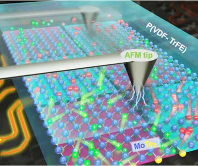
MoTe 2 lateral pnpn homojunction is tuned using a ferroelectric domain controlled by a probe. When the ferroelectric polymer-P (VDF-TrFE) is polarized up and down, electrons / holes are injected into the channel. (Photo: Shanghai Institute of Technical Physics, Chinese Academy of Sciences)
The realization of p and n doping is crucial for manufacturing 2D semiconductor devices with advanced functions. In this work, researchers showed a method of patterning ferroelectric domains doped with 2D materials.
When the conductive probe is scanned on the surface of the ferroelectric thin film with a negative voltage, the ferroelectric thin film is polarized. Iron electrodeization uses the non-volatile nature of the electrostatic field at the interface to dope the underlying MoTe 2. Holes were injected into the MoTe 2 channel to shield the polarization field, creating a p-doped MoTe2.
Similarly, when the ferroelectric film is polarized downward by using a positive scanning voltage, an n-doped MoTe 2 channel can be obtained.
The ferroelectric domain pattern can be written without being restricted by the metal electrode, and can be arbitrarily edited based on the PFM scanning technology. In addition, iron polarization is non-volatile and can be changed by external voltage pulses. This means that the written ferroelectric domain pattern can be erased and rewritten to make new functional devices.
Unlike conventional electrostatic doping, the ferroelectric field formed by the ordered arrangement of dipoles at the interface is non-volatile. The polarization direction of a ferroelectric material can be controlled by a voltage applied to the PFM tip, which acts like a gate electrode in a conventional transistor.
This doping method has its unique charm. Compared to a conventional transistor with a fixed gate electrode, the PFM tip can move freely, thereby releasing the ferroelectric domain pattern restricted by the metal electrode and allowing arbitrary editing.
Based on this cutting-edge scanning technology, the team manufactured electronic and optoelectronic devices such as MoTe 2 pn, np, pp, nn homojunctions, as well as electrical writing and optical reading storage devices.
They also used Fudan University‘s Peng Zhou research team to explore a quasi-nonvolatile memory with the help of a ferroelectric domain mode method. The memory has a refresh time of 100 s and a write / erase speed of 10 μs.
"The next step will be to improve the ferroelectric field by reducing the depolarization field to optimize the stability and durability of the device," Wang Jianlu said.
Source: Provided by Shanghai Institute of Technical Physics, Chinese Academy of Sciences as Nanowerk