(Nanowerk News) A group of researchers from Sungkyunkwan University in South Korea published a paper on NANO ("Heterogeneous Integration of 2D Materials: Recent Advances in Manufacturing and Functional Device Applications") on two-dimensional heterogeneous integration ( 2D) for a comprehensive review. ) The materials come from an extensive library of atomic 2D materials, which have optional material properties, opening up fascinating possibilities for functionally novel device designs.
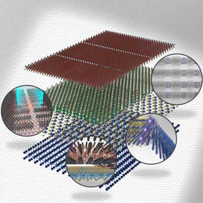
Schematic diagram of emerging heterogeneous integration of 2D heterostructure studies and 2D materials.
Since the discovery of graphene by Andre Geim and Konstantin Novoselov, two-dimensional materials such as graphene, black phosphorus (BP), transition metal carbon disulfide (TMDC), and hexagonal boron nitride (h-BN) have been well received due to their extensive physical properties. attention. Characteristics and wide application in electronic and optoelectronic equipment.
Research on these 2D materials has grown to the point where an extensive library of atomic thin 2D materials with alternative material properties can be created and continues to grow.
By combining or stacking these 2D materials, a 2D heterostructure can be constructed, which is constructed by directly stacking a single single layer containing different materials. Due to the strong covalent bonds between atoms in the single layer, each single layer in the two-dimensional heterostructure is highly stable.
However, the force between the monolayers holding the monolayers stacked on top of each other to form a 2D heterostructure happens to be a relatively weak Van der Waals interaction. Therefore, each single layer retains its inherent characteristics.
Moreover, unlike conventional semiconductor heterostructures, in traditional semiconductor heterostructures, the choice of constituent materials is limited to those with similar lattice structures. Due to the weakening of van der Waals forces, the lattice loss of stacked heterostructures can be relaxed.配 Requirement. This means that despite their different lattice structures, insulating, semiconducting or metallic 2D materials can be combined to form a single 2D heterostructure.
When a single layer is stacked in combination with other single layers made of different materials, various new heterostructures with atomically thin 2D heterojunctions can be created. Heterostructures made from a specific combination of materials will have a specific set of physical properties, depending on which material they are made of. The unusual physical properties of 2D heterostructures make them suitable for a wide range of applications.
In this review, various 2D heterostructures are discussed, and new electronic and optoelectronic properties are explained, advanced synthetic technology developments, and new functional applications available. It provides an understanding of the current research trends of 2D materials, thereby exploring the future possibilities of nanomaterials research.
Source: World Science