 Since the 1940s, the information technology revolution led by microelectronics has greatly promoted the development of science and technology and social changes. In the past few decades, the microelectronics technology industry has made rapid progress along Moore‘s Law. According to Moore‘s Law, the number of transistors that can be accommodated in integrated circuits doubles approximately every two years. The smallest achievable processing size in integrated circuits today is 3-5 nanometers. At present, as the feature size of integrated circuits approaches process and physical limits, further reducing the feature size of transistor devices is extremely challenging.
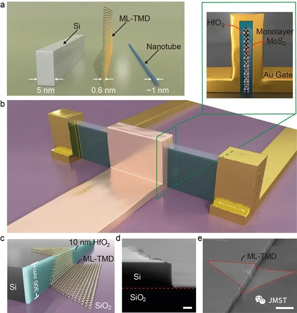
Compared with traditional bulk silicon semiconductor materials, low-dimensional materials with atomic scale have been rapidly developed in recent years. New materials such as carbon nanotubes and two-dimensional atomic crystals are constantly being tried for channel materials or electrode materials for transistors. Recently, researchers from the Shenyang National Research Center for Materials Science, Institute of Metal Research, Chinese Academy of Sciences, cooperated with many units at home and abroad to demonstrate for the first time an arrayable, vertical single atomic layer channel fin field effect transistor (FinFET) (Figure 1). "Nature Communications" published an online research paper entitled "A FinFET with one atomic layer channel".
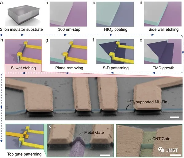
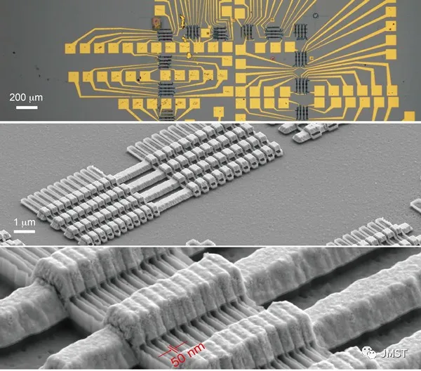
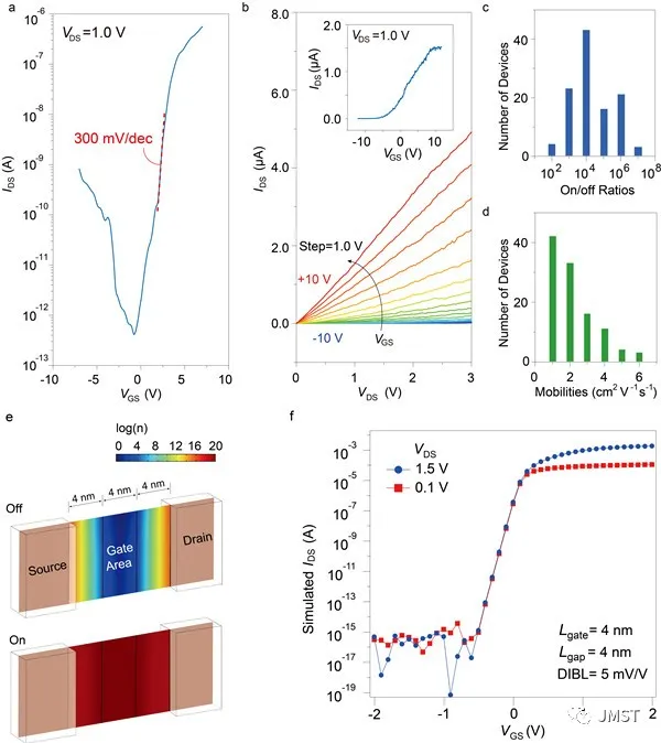
The researchers designed a silicon crystal step template with a height of ~ 300nm, and realized a transition group metal sulfide monoatomic layer crystal (MoS2, WS2, etc.) grown conformally to the side wall of the step by wet spraying chemical vapor deposition (CVD) method. . A fin-type field-effect transistor using a single-layer limiting two-dimensional material as a semiconductor channel was prepared by using a micro-nano processing process such as multiple etching (Fig. 2), and a fin-type field-effect transistor array was successfully prepared (Fig. 3). In addition, attempts have been made to introduce carbon nanotubes to replace traditional metals as gate materials. The results show that the materials have better cladding properties than traditional metal gates and can effectively improve device performance. Through statistical measurement of hundreds of transistor devices, the current switching ratio was measured to be 107, and the sub-threshold swing was 300mV / dec (Figure 4a-d). Theoretical calculations show that the proposed fin-type field effect transistor can achieve excellent resistance to short channel effects, such as the reduction of the barrier introduced by the drain (DIBL) can be as low as 5mV / V (Figure 4e-f).
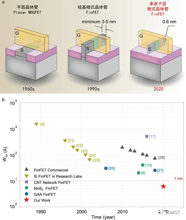
This work reduced the channel material width of FinFETs to the sub-nanoscale (0.6 nm) of the single atomic layer limit (Figure 5). At the same time, a single atomic layer channel fin array with a minimum pitch of 50 nm was obtained. The work provides a new solution for the development of field-effect transistor devices in the post-Moore era.
The work was completed by the Institute of Metal Research of the Chinese Academy of Sciences in cooperation with Hunan University, Shanxi University, Suzhou Institute of Nanotechnology, Chinese Academy of Sciences, Hefei High Magnetic Field Science Center, French Atomic Energy Agency and other units. Han Zheng and Sun Dongming‘s group of the Institute of Metals led the research project, responsible for device preparation and characterization; Liu Song‘s group of Hunan University is responsible for CVD growth; Dr. Dong Baojuan of Shanxi University is responsible for finite element simulation; The carbon nanotube solution for preparing the gate material was prepared; Du Haifeng‘s group at the center of the strong magnetic field led the preparation and characterization of relevant TEM samples. Dr. Maolin Chen, Dr. Xingdan Sun, and Master Liu Hang (Hunan University) are co-first authors, and Han Zheng, Sun Dongming, Liu Song, and Dong Baojuan are co-corresponding authors. This research work was supported by the National Natural Science Foundation of China, the Chinese Academy of Sciences, the National Research Center for Materials Science of Shenyang, the National Key R & D Program Youth Project, and the Youth Thousand Talents Program.

Figure 1: Finned field effect transistor with single atomic layer channel. a) Schematic comparison of the dimensions of channel materials, vertical two-dimensional atomic crystals, and single carbon nanotubes for FinFETs in silicon processes. b) Device structure diagram. The illustration is a schematic cross-section. c) Schematic illustration of a single-layer two-dimensional transition group metal sulfur compound grown in conformal steps. d-e) Scanning electron micrograph of the step template, with scales of 100 nm (left) and 1 micron (right).

Figure 2: Device process flow and SEM photo.

Figure 3: Topography of an arrayable single-atom layer fin transistor (minimum array spacing is 50 nm).

Figure 4: a) -d) Electrical performance of single-atom layer fin field effect transistor; e) -f) Finite element calculation simulation

Figure 5: a) Several configurations of MOSFET field effect transistors; b) Development history of FinFE device fin width.
Information source: jmst


