|
Carbon comes in many different forms, from the graphite found in pencils to the world��s most expensive diamonds. In 1980, we knew of only three basic forms of carbon, namely diamond, graphite, and amorphous carbon. Then, fullerenes and carbon nanotubes were discovered and more recently there has been a lot of buzz about graphene. Discovered only in 2004, graphene is a flat one-atom thick sheet of carbon. Existing forms of carbon basically consist of sheets of graphene, either bonded on top of each other to form a solid material like graphite, rolled up into carbon nanotubes (think of a single-walled carbon nanotube as a graphene cylinder), or folded into soccer ball shaped fullerenes.
|
|
Experiments with graphene have revealed some fascinating phenomena that excite nanotechnology researchers who are working towards molecular electronics. It was found that graphene remains capable of conducting electricity even at the limit of nominally zero carrier concentration because the electrons don��t seem to slow down or localize. This has to do with the fact that the electrons moving around carbon atoms interact with the periodic potential of graphene��s honeycomb lattice, which gives rise to new quasi particles that have lost their mass, or ��rest mass�� (so-called massless Dirac fermions). This means that graphene never stops conducting.
|
|
Taking advantage of the conducting properties of graphene, James M. Tour at Rice University and his team have described how graphene memory could potentially be used as a new type of memory that could significantly exceed the performance of current state-of-the-art flash memory technology.
|
|
"What distinguishes graphene from other next-generation memories, in particular phase-change materials, is its vastly higher on/off power ratio �C the amount of current a circuit holds when it��s on, as opposed to off," Tour explains to Nanowerk. "While the on/off ratios of phase-change materials are generally in the 10-100 region, with graphene it can be as high as a whopping million-to-one or even more �C we have seen as high as 10 million-to-one."
|
|
The transistors currently used in computer chips have on/off ratios of 10,000 - 100,000, but they are three-terminal devices (in a three terminal device the electric current or voltage between two of the terminals is controlled by applying an electric current or voltage to the third terminal). Two-terminal memories based for instance on nanowires or carbon nanotubes are actively researched for future computer applications. Their structure makes three-dimensional memory practical as the materials can be stacked, multiplying a chip��s capacity with every layer. The main challenges so far have been a requirement for large-scale fabrication and reliable and large on/off ratios.
|
|
The recent research results coming out of Tour��s lab show the possibility of building next-generation memory devices with vast amounts of memory using nanocables with a silicon dioxide core and a shell of stacked sheets of graphene (the team experimented with three different nanocable configurations: two layer graphite/silicon dioxide and three-layer graphite/silicon dioxide/silicon and graphite/silicon dioxide/ silicon carbide). Tour points out that graphene memory would increase the amount of storage in a two-dimensional array by a factor of five, as individual graphitic thin film sheets could be made as thin as 5-10 nanometers, compared to the 45-nanometer circuitry in today��s flash memory chips.
|
|
Tour, together with postdoctoral researchers Yubao Li and Alexander Sinitskii, describes a solid-state device that takes advantage of the conducting properties of graphene in the November 16, 2008 online edition of Nature Materials ("Electronic two-terminal bistable graphitic memories").
|

|
|
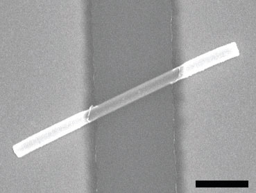
SEM image of a G�CSiO2 nanocable two-terminal device. Scale bar = 250 nm (Reprinted with permission from Nature Publishing Group)
|
|
When the scientists tested their nanocable devices in the lab, they observed not only excellent endurance �C the nanocables showed no degradation after more than 1,000 write�Cread�Cerase�Cread cycles �C but also no discernable data loss even after weeks of testing, sometimes under harsh temperature conditions that ranged from minus 70��C to plus 200��C.
|
|
"Interestingly, the devices were also stable to ionizing radiation," says Tour. "In our experiments, we irradiated the unbiased devices with a high dose (>20 Mrad) of 8 keV X-rays, which was significantly higher than the typical failure level for memory devices relying on charge storage, such as flash memories. Thus, nanocable memories demonstrate exceptional stability and are promising for radiation-stable electronics."
|
|
The Rice team claims that the new switches are faster than their lab��s current testing systems can measure (1 microsecond), although they observed that the write/erase time affected the on/off ratio: "The longer the time, the higher the on/off ratio" says Tour. "When decreasing the pulse time from 100 microseconds to 1 microsecond, the on/off ratio in graphite/silicon dioxide nanocable devices decreases to about 100."
|
|
Tour��s lab is already working on developing scalable manufacturing techniques for their nanocable device. According to Tour, it is possible to deposit a layer of graphene on silicon or another substrate by chemical vapor deposition. "This means that currently used industrial device fabrication processes could be used to grow this type of graphitic thin film in place."
|
|
An important aspect that Tour describes in his paper is the fabrication atop a silicon wafer in a manufacturable-looking structure. This is essential because nanowires are hard to scale into manufacturable structures since they are tough to place where you want them. Tour��s technique shows a way of how to build these future device structures.
Source: nanowerk
|


