|
Getting from 2D to 3D has been quite a challenge for the graphene community. The transfer of two-dimensional graphene onto three-dimensional surfaces has proven to be difficult due to the fractures in graphene caused by local stresses. Although researchers have investigated the integration of graphene onto microstructured surfaces (see for instance: "A universal and rapid method for transferring nanostructures" and "Ultraflat transfer method for graphene surface force balance"), the damage-free nature of graphene around the 3D structures has not been previously demonstrated.
|
|
New research coming out of the University of Illinois at Urbana-Champaign is bound to change that. A team, led by SungWoo Nam, an Assistant Professor in the Department of Mechanical Science and Engineering, has demonstrated graphene integration into a variety of different microstructured geometries �C pyramids, pillars, domes, inverted pyramids, as well as the integration of hybrid structure of graphene decorated with gold nanoparticles on 3D structures.
|
|
The team reported their findings in the June 18, 2015, online edition of Nano Letters ("Three-Dimensional Integration of Graphene via Swelling, Shrinking, and Adaptation").
|

|
|
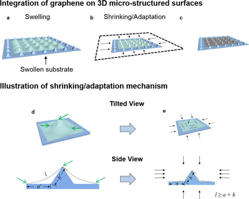
Schematic illustration of the 3D integration of graphene. (a) Graphene with supporting layer transferred onto a 3D swollen PDMS substrate. The graphene with supporting layer is suspended (i.e., not conformed to the substrate). (b) PDMS substrate shrinking during the evaporation of solvent (e.g., toluene). Three-dimensional adaptation of graphene/supporting layer is achieved through this step. (c) Removal of the transfer film with a proper etchant (e.g., acetone for PMMA). (d) Detailed schematics of (a). Graphene is adhered to the nearby planar region of the pyramid and the top of pyramid, acting as anchoring points (green arrows). Graphene is not conformed and suspended around the pyramid. l is the length of suspended graphene, and a�� and b�� are the lengths of planar region and pyramid under the suspended graphene, respectively. (e) Detailed schematics of (b). During shrinkage, 3D adaptation of graphene onto pyramid is achieved and a few small wrinkles/crumples of graphene emerge. a and b indicate the final lengths of planar region and pyramid under the graphene after the substrate shrinkage. Black arrows indicate shrinking directions. (Reprinted with permission by American Chemical Society) (click on image to enlarge)
|
|
"We demonstrate a fully conformal 3D integration of graphene via substrate engineering," Nam tells Nanowerk. "To avoid damage to graphene from tensile and/or capillary stress and to achieve uniform integration onto 3D microstructured surfaces, we developed three sequential steps: substrate swelling; shrinking; and adaptation."
|
|
"Our method utilizes wet-transfer and adaptive substrate-engineering, providing several key advantages over other fabrication/integration methods of 3D graphene," explains Jonghyun Choi, a graduate student in Nam��s research group and first author of the paper. "First, we transferred graphene with a 50nm PMMA transfer film onto a swollen PDMS substrate, where the transferred PMMA/ graphene is initially suspended on the 3D features �C rather than making conformal contact to the substrate. As the substrate shrinks during the evaporation of the solvent used to swell PDMS, the suspended structure gradually integrates onto the underlying 3D substrate, achieving a 3D adaptation. Finally, we gently removed the transfer film by using the appropriate etchant solution, resulting in 3D integrated graphene with the predesigned substrate."
|
|
"Suspended graphene is prone to damage from tensile and capillary stresses generated between the graphene and substrate during the PMMA removal and subsequent solvent drying processes," adds Nam. "We therefore optimized our swelling, shrinking, and adaptation steps in order to minimize the degree of graphene suspension around the 3D microstructures and facilitate successful 3D integration."
|
|
In order to enhance the integration yield and reduce unwanted wrinkling, the team optimized the amount of substrate swelling and the thickness of transfer film �C which are the two critical integration parameters of this technique.
|

|
|
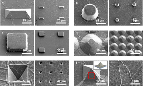
Demonstration of the versatility of 3D integration. (a-e) SEM images showing results of graphene integration onto (a) elongated pyramids, (b) circular pillars, (c) rectangular pillars, (d) domes, and (e) inverse pyramids. (f) SEM images of AuNPs/graphene hybrid structure integrated on pyramid substrate. The right panel shows the magnified image of the red dashed square in the left, demonstrating that there are AuNPs on the walls of the pyramid. (Reprinted with permission by American Chemical Society) (click on image to enlarge)
|
|
The team demonstrated the robust nature of their 3D integrated graphene with scanning electron microscope and atomic force microscope, where the out-of-plane dimensions of the microstructure features spans from a few microns to 50 microns.
|
|
According to the researchers, this fabrication technique can be used to develop active biosensing devices, as the flexibility and 3D nature of the structure conforms to the mechanical characteristics and multidimensionality of biological systems.
|
|
This novel strategy can also be applied to 3D electrodes array for electrophysiological studies of electrogenic cells/tissues.
|
|
In addition, it could solve the challenges associated with graphene integration with various microelectromechanical systems (MEMS).
|
|
Going forward, Nam��s team will investigate the integration of other low-dimensional nanomaterials �C e.g., transition metal dichalcogenides monolayers �C and stretchable 3D electronics and bioelectronics. For example, heterogeneous strain engineering of 2D materials by this 3D transfer method can be used towards novel optoelectronic, metamaterial, and thermoelectric applications.
|


