【introduction】
In the history of human civilization, material science has always been one of the main driving forces driving the development of social productive forces. Especially in the past few decades, various silicon-based devices have witnessed the development and prosperity of the modern information industry, especially in the fields of electronics and optoelectronics. In today‘s society, people urgently need to develop a series of brand-new materials to promote the slowing down of silicon-based device process development. The two-dimensional material family is considered to have huge development potential because of its following advantages: (1) atomic thickness, which can overcome the key short-channel effect, so that the device can reduce power consumption while reducing the size; (2) A variety of excellent properties, such as ultra-high carrier mobility, ultra-fast charge transfer between interfaces, etc .; (3) With a complete basic unit of devices such as conductors, semiconductors, insulators, magnets, etc., it can be prepared Logic, storage, photoelectric and photonic devices; (4) Compatible with the processing technology of traditional silicon-based devices, which can quickly realize the scale and high integration of two-dimensional devices. However, in order to truly develop the huge potential of high-concentration applications for two-dimensional devices, we must first break through the technical difficulty of preparing large-scale two-dimensional single crystals. Because only large-sized two-dimensional single crystals can provide extreme material performance with high consistency, and can also avoid material performance degradation caused by defects and grain boundaries, which is critical to the high integration of the device. Therefore, it is very important to study the growth of large-scale two-dimensional single crystals. However, many successful experiences in traditional three-dimensional single crystal growth cannot be directly applied to the preparation of two-dimensional single crystals, mainly because two-dimensional materials are only atomically thick, and their growth must depend on the substrate. The controlled growth of the two-dimensional single crystal is mainly based on the surface and interface regulation between the material and the substrate. So far, only graphene and hexagonal boron nitride (hBN) have been prepared as single crystals on the order of meters. Therefore, at this stage, summarizing existing research results and making a more systematic and in-depth understanding of the growth of two-dimensional single crystals can lay the foundation for more controlled growth of two-dimensional single crystals in the future.
【Achievement Introduction 】
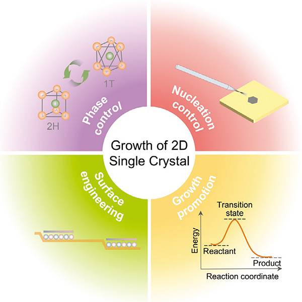
Recently, Kaihui Liu of Peking UniversityResearchers (corresponding authors) and others reviewed and proposed four key factors in the process of controlled growth of two-dimensional single crystals, namely nucleation control, growth promotion, surface regulation, and hybrid phase suppression. Nucleus control and growth promotion are the key factors for the growth of a single nucleus to form a large-sized two-dimensional single crystal. The surface adjustment can make all crystal domains have the same orientation, and then seamlessly spliced into a large-size single crystal film. The goal of heterophasic suppression is to increase the phase purity of the product, thereby obtaining higher single crystal quality. Based on the existing research results, the author has made a more systematic and in-depth understanding of the growth of large-scale two-dimensional single crystals. At the same time, the author also discusses the potential growth control methods and application prospects of 2D materials, highlighting the bright future of 2D single crystal material systems. Relevant research results to " the Designed 2D Growth of Large-Size Single Crystals " was published in Adv. Mate r . On.
【Graphic introduction】
Figure 1. Two-dimensional single crystal growthFour keysSchematic diagram of factors
FIG Second, as nucleation control system

(A) Schematic diagram of graphene growth on the surface of liquid Cu;
(B) The corresponding SEM image of graphene;
(C) Schematic diagram of the process in which melamine inactivates the Cu active center, thereby inhibiting the nucleation density;
(D) SEM images with significantly reduced nucleation density of graphene;
(E) Schematic diagram of the design for controlling single-core growth on Cu 85 Ni 15 substrate;
(F) Optical photo of single crystal graphene grown from a single core;
(G) Schematic diagram of graphene evolution selective growth;
(H) 1-foot-long optical photo of single crystal graphene.
Figure 3.Growth promotion

(A, b) STM simulation image of Ni atoms at the edge of graphene;
(Ce) Schematic diagram of graphene edge growth under aerobic and anaerobic conditions and corresponding DFT calculation;
(F) Schematic diagram of local oxygen-assisted catalytic growth;
(Gi) Schematic diagram and corresponding energy curve of methane decomposition reaction process with and without oxygen assistance;
(Jl) Schematic diagram of a possible carbon source decomposition reaction path and corresponding energy curve under the local fluorine-assisted catalysis.
Figure 4. Surface regulation

(A) Optical graph of graphene crystal domains with uniform growth orientation on Cu (111);
(B, c) Low energy electron diffraction pattern of single crystal graphene and Cu (111);
(D) Atomic force microscope (AFM) images of MoS 2 with uniform orientation grown on hBN sheets ;
(E) Fast Fourier transform (FFT) diffraction points of MoS 2 / hBN heterostructure;
(F) The hBN domains grown on Cu (102) with the same orientation, and the background color is the electron backscatter diffraction (EBSD) pattern of the substrate;
(G) Energy calculation of various hBN domain orientations on Cu (102);
(H, i) Schematic diagram of the self-calibration rotation growth of hBN on liquid gold;
(J) hBN crystal domains with uniform orientation on large-sized Cu (110);
(K, l) Low energy electron diffraction patterns of hBN and Cu (110);
(M) Atomic resolution STM images of hBN and Cu (110);
(N) Calculate the energy curve for hBN growth in different orientations using first-principles DFT.
Figure 5. Miscellaneous phase suppression
(A) Schematic diagram of plasma-induced phase transition of MoS 2 from 2H phase to 1T phase;
(B) Atom-resolved STM images during the phase transition of MoS 2 ;
(C) Schematic diagram of phase selection of 2H-MoTe 2 during boundary recrystallization;
(D) The generated 1T ‘phase MoS 2 ;
(E, f) Atomic resolution STEM image and corresponding FFT of the synthesized 1T ‘phase MoS 2 ;
(G) MoS 2 with a schematic view of the policy and the selective growth of K X MoS 2 relationship is formed with the energy difference of the concentration of potassium;
(H) K x MoS 2 growth MoS 2 phase diagram related to H 2 concentration and growth temperature .
【summary】
In summary, this article reviews and discusses the four key factors in the controlled growth of two-dimensional single crystals. At this stage, of all the two-dimensional materials, only graphene and hBN have achieved single-meter crystals on the order of meters through the growth of the substrate surface. Therefore, designing a substrate with appropriate symmetry and preparing it into a large-size single crystal may be a feasible method to achieve large-scale production of two-dimensional single crystal. In addition, the prepared two-dimensional single crystal can be used as a substrate, and the two-dimensional single crystal can be grown again on the surface by the method of interlayer coupling, so as to construct a multilayer two-dimensional single crystal with a controlled number of layers and orientation or a vertical质 结构。 Quality structure. At the same time, some functional nanomaterials with controllable layer number and morphology can also be prepared using two-dimensional single crystal templates. At this stage, the growth of two-dimensional single crystals also has huge research space and potential. In the future, it is expected to realize the development and application of highly integrated full two-dimensional devices based on the preparation of multiple two-dimensional single crystals and their complex heterostructures.
Literature link: " Designed Growth of Large-Size 2D Single Crystals " ( Adv. Mater., 2020 , 10.1002 / adma.202000046)
Source of information: Material cattle


