introduction
Metal halide perovskite materials have the advantages of high absorption coefficient, high diffusion length, and adjustable band gap. They are important candidates for next-generation low-cost, high-performance optoelectronic materials, and have attracted extensive research interest. Perovskite materials can be deposited in multiple steps through the current mature and efficient preparation technology (such as spin coating, spray coating or inkjet printing), effectively overcoming the complicated preparation process of traditional inorganic materials (such as silicon, germanium and gallium arsenide) , High cost and other shortcomings, provides an effective alternative way to achieve low-cost, industrial preparation. Although considerable progress has been made in the research on the mechanism and performance optimization of perovskite materials in recent years, due to the inherent water-oxygen instability of perovskite materials, imaging arrays based on perovskite materials currently face great Process difficulties, including: material synthesis, device miniaturization and integration, etc. At the same time, the currently reported methods for preparing perovskite imaging arrays are based on methods that strictly control the growth of materials. Such methods require strict processes, making it difficult to achieve stable, high-quality factor large-area array devices. Therefore, it is extremely important to develop a controllable patterned preparation technology for perovskite materials. In addition, if there is a mismatch between the Fermi level of the perovskite material and the work function of the electrode, the carrier transport efficiency will be reduced, thereby reducing the device performance. For the manufacture of photoconductors and transistor detectors, achieving ohmic contact is very important for studying the intrinsic properties of materials and mentioning the performance of devices. Therefore, another key issue currently facing is how to between the perovskite material and the electrode material Form a good ohmic contact. MXene is an emerging two-dimensional material. Due to its unique two-dimensional structure, it has special chemical properties and surface co-functional groups. It exhibits excellent material properties, such as: approximate metal conductivity, chemical stability, mechanical Elasticity, good solution dispersion and adjustable work function (1.6-6.2eV). This adjustable work function makes MXene an ideal material for forming good ohmic contact with various semiconductor materials. In addition, MXene can also be dissolved and prepared under low temperature and air atmosphere, thus enabling a fast, low-cost, complementary metal oxide semiconductor (CMOS) compatible manufacturing process.
Achievements
Recently, Professor Wu Jiang, University of Electronic Science and Technology and Professor Zhao Dewei Sichuan University reported a technique by laser direct-write method to achieve the absorption layer of the detector array based MXene electrode and the perovskite, which avoids complex process lithography, effective Solved the problem of miniaturization and patterning of perovskite film and MXene electrode. At the same time, combining the advantages of MXene and perovskite materials that can be prepared by solution method, a photoelectric detector array with a large area array of 1250 pixels was developed. The device has wide-band spectral response capability from visible to near infrared (400-810 nm), high response rate (84.77 AW -1 ), high detection rate (3.22 × 10 12 Jones) and excellent linear dynamic range (82 dB) A demonstration of near infrared imaging is realized. This work provides a new idea for the development of a new generation of low-cost, large-area array and high-performance photodetector imaging arrays. The result was published in the internationally renowned journal Materials Horizons as "Direct laser-patterned MXene-perovskite image sensor arrays for visible-near infrared photodetection" .
Photo REVIEW Figure
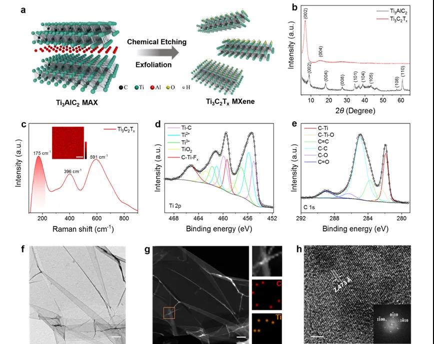
A Ti 3 C 2 T x MXene structure and morphology characterization

(a) Synthesis and structure diagram of Ti 3 C 2 T x MXene;
(b) XRD pattern of Ti 3 AlC 2 MAX powder and few layers of Ti 3 C 2 T x MXene film;
(c) Raman spectrum of a few Ti 3 C 2 T x MXene films;
(D) Ti 2p and (e) XPS spectra of Ti 3 C 2 T x MXene thin film with few layers ;
(f) Bright field TEM image of single layer Ti 3 C 2 T x MXene nanosheets;
(g) Dark-field TEM, STEM-HAADF, and EDS images of single-layer Ti 3 C 2 T x MXene nanosheets;
(h) HR-TEM image of single-layer Ti 3 C 2 T x MXene nanosheets.
Fig. 2 Characterization of energy band structure of Ti 3 C 2 T x MXene and CsFAMAPbIBr perovskite

(a) UPS energy spectrum near the secondary electron cut-off transformer;
(b) UPS energy spectrum near Fermibian;
(c) PL spectrum of CsFAMAPbIBr perovskite and ( αhν ) 2 - hν curve;
(d)-(g) Schematic diagram of work function arrangement and carrier transport.
Figure 3 Preparation process and device structure of the detector array

(a) Flow chart of preparing MXene-perovskite detector array based on solution method and laser direct writing;
(b) A detector array with 25x50 pixels;
(c) Photoconductive pixel unit structure;
(d) Microscopic image of device pixel unit.
Fig. 4 Broad-spectrum optical response characteristics of the device

(a) Visible-near infrared (405-808 nm) IV characteristic curve ;
(b) Visible-near-infrared (405-808 nm) wavelength changing light intensity switching characteristics;
(c) Simulation curve of device near infrared interference enhanced absorption;
(d) Simulated battery mode distribution of device cross-section.
Figure 5 Device performance characterization and infrared imaging demonstration
(a) Transient optical response curve of the device;
(b) Linear dynamic range at visible-near infrared (405-808 nm) wavelength;
(c) Response rate and detection rate at visible-near infrared (405-808 nm) wavelength;
(d) Demonstration of imaging of 808 nm near infrared light pattern by detector array;
(e) The performance of the detector array is compared with the pixel level.
summary
In summary, this paper proposes a laser direct writing method to prepare a large-area array MXene-perovskite detector array. Combining the advantages of the two materials in the energy band structure and the solution method preparation, the MXene electrode and the perovskite absorption layer can be directly processed from large to small scales to solve the graphic problem of the perovskite device A COMS compatible full solution preparation process is introduced. Thanks to the good energy level matching between the two materials and the enhancement of near-infrared interference, the device obtains a broad-spectrum response capability of visible-near infrared (400-810 nm), and a high response rate (84.77 AW -1 ) Detection rate (3.22 × 10 12 Jones) and excellent linear dynamic range (82 dB). At the same time, the large area array device with 1250 pixels realized good image capturing function under 808 nm near infrared light. This work will provide innovative solutions for the design and processing of next-generation low-cost, large-area array and high-performance perovskite-based detector arrays.
Article link: Direct laser-patterned MXene-perovskite image sensor arrays for visible-near infrared photodetection. Mater. Horiz., 2020 , DOI: 10.1039 / D0MH00537A.
Source of information: material person


