已传文件:photo/20208593750450.png
Abstract: Nano-optoelectronic devices are becoming the core of next-generation optoelectronic devices. The article introduces the application of micro-nano processing technology represented by electron beam lithography and inductively coupled plasma etching in optoelectronic devices, including quantum dot lasers, quantum dot THz detectors and photonic crystal devices.
Keywords: nano-optoelectronic devices; electron beam lithography; inductively coupled plasma etching; quantum dot devices; photonic crystals
1 Introduction
In the past 50 years, the progress of micro-nano processing technology has greatly promoted the development of microelectronic technology and optoelectronic technology. The development of microelectronics technology is represented by very large-scale integrated circuits, and the integration rate is increasing at a rate of doubling every 18 months, so that integrated circuit chips with a minimum circuit size of 90nm have begun mass production. Take photolithography and etching as The basic planar processing technology has become the core technology of VLSI. With the emergence of electron beam lithography and inductively coupled plasma (ICP) etching technology, planar micro-nano processing technology is promoting the integration of single electronic devices and automatic The development of a new generation of nanoelectronics represented by gyroelectronic devices. When micro-nano processing technology is applied to the field of optoelectronics, emerging nano-optoelectronics technology has been formed, mainly studying the interaction of light and electrons in nanostructures and the technology of energy exchange .Nano-optoelectronic technology in the past ten years, on the one hand, nano-manufacturing technology based on low-dimensional structure material growth and energy band engineering has made great progress, including molecular beam epitaxy (MBE), metal organic chemical vapor deposition Product (MOCVD) and chemical beam epitaxy (CBE), so that the epitaxial layer on the wafer surface epitaxial growth direction (straight direction) precision is controlled to a single atomic layer, thereby obtaining a semiconductor material with quantum size effect; on the other hand, planar nano The processing technology realizes nano-scale lithography and lateral etching, making it possible to produce artificial lateral quantum confinement quantum wires and quantum dots. At the same time, the emergence of the concept of photonic crystals makes nano-planar processing technology widely used in optical media materials The refractive index is changing periodically.
This article will focus on the application of electron beam lithography and ICP etching technology in emerging nano-optoelectronic devices, including quantum dot lasers, quantum dot THz detectors and photonic crystal devices.
2 Electron beam lithography technology
Electron beam lithography is a technology that uses electron beams to directly draw or project and copy patterns on a wafer coated with electronic resist [2]. Electronic resist is a polymer that is sensitive to electrons. The scanned electronic resist undergoes molecular chain reorganization, which changes the chemical properties of the resist in the exposed pattern. After developing and fixing, a high-resolution resist exposure pattern is obtained. The main process of electron beam lithography technology is glue coating, pre-baking, electron beam exposure, development and hardening. Modern electron beam lithography equipment has been able to produce fine line structures less than 10nm. Electron beam lithography equipment is also an important tool for making optical masks.
The internal process factors that affect the exposure accuracy mainly depend on the electron beam spot size, scanning step length, electron beam dose and proximity effect caused by electron scattering. The higher the energy of the electron beam, the smaller the diameter of the beam spot. For example, the diameter of the electron beam spot at 10keV is 4nm, and it is reduced to 2nm at 20keV. The scanning step length of the electron beam is limited by the beam spot diameter. If the step length is too large, it is impossible to realize the compact plane beam scanning; if the step length is too small, the electron beam scanning area will be subjected to excessive electron scattering. The electron beam dose is determined by the beam current intensity and residence time. If the dose of the electron beam is too small, the resist cannot be fully photosensitive; if the dose of the electron beam is too large, the resist at the edge of the pattern will suffer excessive electron scattering. Since the wavelength of high-energy electrons is hundreds or thousands of times shorter than the wavelength of light, it is not the diffraction of electrons that limits the resolution, but the various electronic astigmatisms and the scattering of electrons in the resist. The electron scattering will reduce the electron energy and dose on the inner side of the pattern edge, resulting in an inner proximity effect; at the same time, the scattered electrons will make the resist on the outer side of the pattern edge photosensitive, resulting in an outer proximity effect. The inner proximity effect rounds the corners of the vertical graphics, while the outer proximity effect makes the edges of adjacent graphics approach and blur.
The external process factors that affect the exposure accuracy include the thickness of the electronic resist and the development time. The thinner the electronic resist, the higher the resolution of the exposed pattern, but the masking effect will be reduced. The longer the development time, the less clear and even extended the edges of the graphics. In addition, ambient temperature, electromagnetic interference, mechanical vibration and unstable power supply will affect the exposure accuracy.
Electron beam lithography can directly produce the required patterns under the control of a computer. Since the electron beam deflection field (that is, the writing field) is very small, usually 100-1000 μm2, the electron beam exposure pattern is spliced by the writing field, as shown in Figure 1. After the electron beam scans a writing field, the laser-controlled worktable moves the next adjacent area into the electron beam scanning range according to instructions. Therefore, writing field alignment is a key step to determine the accuracy of pattern splicing. For the first exposed pattern, the write field alignment actually defines the direction and sequence of the electron beam scanning as parallel to the xy movement direction of the table plane defined by the edge of the wafer. For pattern engraving, the writing field alignment is to define the direction and sequence of electron beam scanning as parallel to the xy movement direction of the worktable plane defined by the engraving mark. The write field splicing error of modern electron beam lithography equipment has reached 30-60nm. Try to put the exposed graphics in the same writing field. For graphics larger than the writing field, avoid key parts of the graphics at the boundary of the writing field. Generally, the larger the writing field, the greater the electron beam deflection, the stronger the electron scattering, and the lower the exposure accuracy.
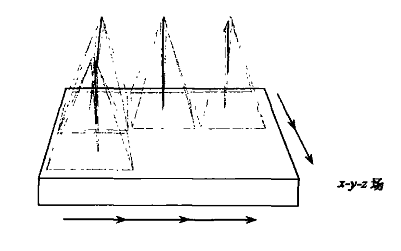
Figure 1. Writing field stitching during electron beam exposure
......
5 Conclusion
The development of micro-nano processing technology will promote the development of nano-optoelectronic devices in a deeper and broader direction. Micro-nano-machined semiconductor nanostructures bring many new quantum physical effects in the field of optoelectronics, such as the Coulomb blockade effect of quantum dots and photon-assisted tunneling effect, and the photonic band gap effect of photonic crystals. Research on the new phenomena brought about by these new nanostructures will lay the foundation for the development of new devices based on new principles.
This information is sourced from the Internet for academic exchange only. If there is any infringement, please contact us to delete it immediately.