已传文件:photo/202081591247121.png
Recently, in the circle of friends in the semiconductor industry, it has been hotly reported that a giant in order to realize IDM digging talents to build a lithography machine, now it is a real hammer. Of course, some self-media still want to beep again in order to conceal their previous suspicions, but they can only be a man with a man‘s arm as a car. However, its beeping still cannot hinder the giant‘s pace and IDM‘s vision.

Rumors about domestic lithography machines circulating online recently
Since the technology threshold and patent bottleneck of the lithography machine in the era of silicon-based chips are so high, how should we achieve corner overtaking?
For chips, the more crystals in the same type of volume, the stronger the performance, which is determined by Moore‘s Law. It is also a high-end nanotechnology goal pursued by both domestic and foreign chip design and processing manufacturers.
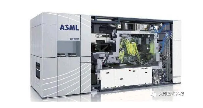
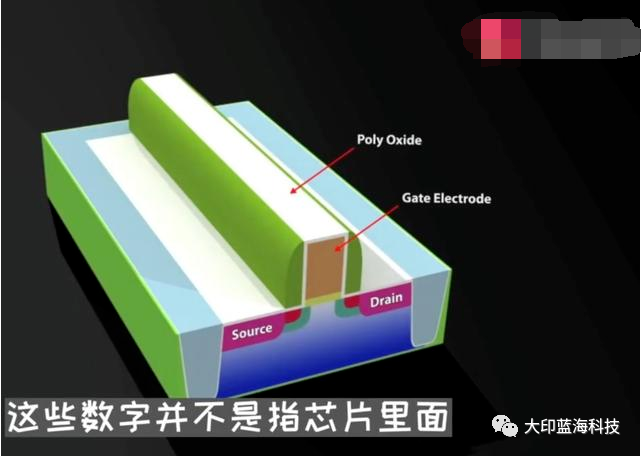
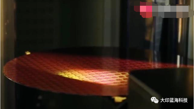
Lithography machine is one of the most important tools for making chips. Those 5nm, 7nm, 10nm, 14nm, etc. on the market do not talk about the number of transistors in the chip, but the size of the transistors in the chip. If you want to make smaller transistors, right The light source and lens on the lithography machine have extremely high requirements. According to the principle of [speed of light = frequency × wavelength], the smaller the wavelength, the higher the frequency. When the frequency is higher, the transmission path of ultraviolet rays is straighter, the jitter is smaller, and the pixel points of the image will be denser and smaller. At present, only the EUV lithography machine of ASML in the Netherlands can do it, and the wavelength of its extreme ultraviolet light source is 13.5nm.
China’s development in the era of silicon-based chips was relatively late, and as netizens said, it was led by the nose to make progress. After so many years, there have been few breakthroughs. Until now, when silicon transistors are about to reach their limits, our Chip nanotechnology is still breaking through the 7nm process, so is there a new way to improve the performance of the chip without using such a high-level nano process? The answer is yes. This is the carbon-based chip using carbon nanotubes as the material discussed in this article.
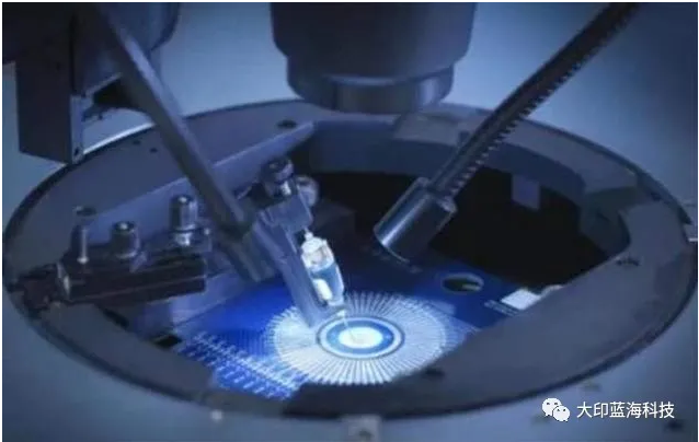
So will carbon-based chips still rely on high-end ASML high-end lithography machines? Definitely not. After all, the purpose of our research and development is to get rid of the control of ASML high-end lithography machines and create our own new material chip era. Because the specific production process did not reveal the news, but it must be, even if a lithography machine is needed To characterize the circuit, a domestic lithography machine is sufficient. The development history of silicon-based chips is very long, and the technology of carbon-based high-end chips has just begun. Due to the characteristics of silicon-based materials, there are tens of billions of transistors in a current ordinary chip, so its power consumption will be It becomes higher, the heat becomes larger, and the probability of failure increases accordingly. Moreover, the process of mounting tens of billions of transistors in a chip less than 1 cm is very complicated, and many countries cannot do it.
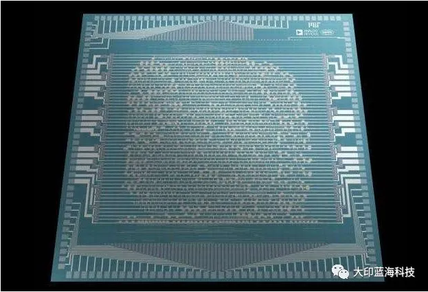

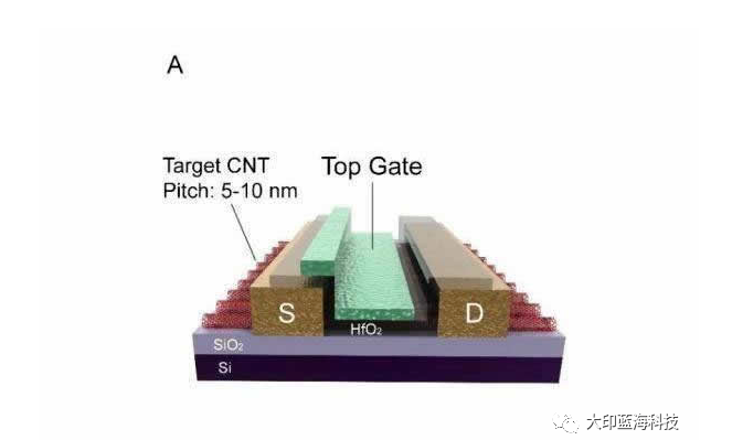
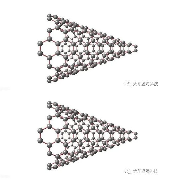
To break this dilemma, it is necessary to abandon traditional silicon materials and use carbon. The electron mobility of transistors made of carbon nanotubes is 1,000 times that of silicon, and the electronic activities in the carbon materials are more free and not easy to generate heat by friction. Transistors using carbon nanotubes as raw materials have more than 10 times the performance of silicon-based chips with the same gate length. This will greatly improve the performance of future carbon-based chips and reduce heating power consumption.

Carbon-based chips have lower power consumption, stronger performance and higher stability than silicon-based chips with the same gate length, and also have their unique characteristics-stretchability. This also means that in the future market applications will become more extensive, such as our smart wearable devices, folding mobile phones, etc., the current mobile phone screen has overcome the flexible screen and curved screen technology, but because of the current hardware, folding Expensive hinges are also needed in screen mobile phones, which is both inconvenient and costly. If the internal circuits and chips can be made of carbon nanotubes, it means that the stretchability will be better, and the silicon-based chips are around 2nm. , Every time the process is improved is a massive investment.
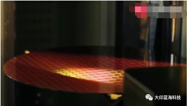
With the efforts of Professor Zhang Zhiyong and Professor Peng Lianmao of Peking University and their team, they have developed a new method of storage and assembly, and have produced 99.9999% high-purity, high-density carbon nanotube materials for semiconductor arrays. However, carbon-based material chips are limited by current materials and technologies. If they want to be commercialized, it will take at least 3-5 years. If you want to mass produce, it is estimated that it will be 10 years later.


As with 5G technology, in the development of carbon-based chips, whoever takes the first step to make a breakthrough will have priority in obtaining patent rights and control rights. The development of a product is based on countless breakthroughs and patents. The investment in carbon-based chips is not only In terms of cost and personnel, the research and development of carbon-based chips is just the beginning. If you want to apply them to various platforms in the future, you will need to adapt to other hardware and software. This will require a large number of developers to conduct research and explore. But one thing is that carbon-based chips must be an important goal for my country‘s future chip development.
As the world‘s advanced chip manufacturer TSMC, it has broken through the 5nm process in the research and development of silicon-based chips, and is moving towards the 2nm process, but after 2nm, the process of silicon-based chips seems to have encountered a bottleneck. However, because my country has been sanctioned by the United States, although it has achieved some achievements in chip design, it cannot break through in manufacturing equipment such as lithography machines. Under the trend of the two situations, scientific and technological personnel all over the world began the research and development of new material chips.
Does carbon-based chip need a photolithography machine
To be sure, carbon-based chips do not require a photolithography machine, so photoresist will n
 ot be used. Otherwise, if Professor Peng Lianmao and Zhang Zhiyong spend so much energy to develop carbon-based chips and rely on photolithography machines, Then its use value is not high. After all, in the research and development of lithography machine, the gap between us and ASML is still very large, so if you want to overtake in a corner, you must get rid of the control of the lithography machine. Moreover, the current silicon-based chips have developed to 2nm technology, which has basically reached the bottleneck. It will be very difficult to continue to break through, so the development of a new material of chips has become a common goal of the world‘s technology industry. However, in this step, we came earlier.
The production process of ordinary chips
The manufacturing process of traditional chips requires a series of complex processes such as polishing, photolithography, etching, and ion implantation. That is, first use a laser to engrave the circuit on the masking plate (equivalent to our printing transfer technology), and then use violet light to print the circuit on the silicon wafer through the masking plate for exposure, and then apply photoresist and other etching. Hundreds of millions of transistors are manufactured on the silicon circle, and finally the packaging and testing are performed, and the chip is completed. And this process cannot leave the lithography machine and the etching machine.
Carbon-based chip manufacturing process
The carbon-based semiconductor chip uses carbon nanotubes or graphene. The preparation process of carbon nanotubes and graphene is essentially different from the preparation method of silicon-based transistors. The main raw material of the two is graphite. The current production process can be passed It is made by various methods such as arc discharge method and laser ablation method. Therefore, the processing of carbon-based chip circuits will definitely not use lithography machines.

What are the advantages of carbon-based chips compared to silicon-based chips
Carbon-based chips using the graphene manufacturing process can reach more than 10 times that of ordinary silicon-based chips, and will continue to promote the better development of Moore‘s Law. Even if the silicon-based chip process breaks through 5nm and reaches 2nm, it will not break through the improvement of 10 times. . Such ultra-fast speed is due to graphene and carbon nanotubes, which have better conductivity in signal transmission.

The carbon-based chip is a revolution in the chip industry. It will break the traditional chip market and redefine what a smart chip is. In addition, the production process does not require the use of lithography machines and photoresist equipment, which will also allow Our country is stuck by these two devices. Now the only thing we can do is to make every effort to promote the development of carbon-based chips. This is the new development goal of our chip industry.
How long does it take to overtake a corner

Whether it is the processor CPU of a mobile phone or various other microcircuit chips, my country‘s production technology and manufacturing equipment must lag behind the international level, and it is difficult to surpass it in a short time. However, the successful research and development of carbon-based semiconductors can enable my country to achieve corner overtaking in the chip field, reaching the international advanced level. Professor Peng Lianmao said:
"The biggest problem facing the manufacture and commercialization of carbon nanotubes is determination. The country‘s determination. If the country provides support for traditional integrated circuit technology, coupled with the full support of the industry, there should be commercial carbon-based technology in 3-5 years. With the emergence of chips, carbon-based chips will begin to enter high-end, mainstream applications within 10 years."

to sum up
It is believed that in the near future, through the adaptation and research and development of various domestic manufacturers, my country‘s carbon-based chips can once again become the world‘s leader and get rid of the state of being stuck by the photolithography machine and photoresist. Seize control of the carbon-based chip industry. At that time, we can have enough voice in the international market, and with the development of carbon-based chips, China’s intelligent equipment will also be significantly improved. This improvement is not only in our mobile phones and digital products. Even in important fields such as military and aviation will usher in new breakthroughs.
Donation is not worthy of contributions, Yuru Yucheng, pay tribute to China Semiconductor Manufacturing!
This information is from the Internet for academic exchange only, if there is any infringement, please contact us to delete it immediately


 ot be used. Otherwise, if Professor Peng Lianmao and Zhang Zhiyong spend so much energy to develop carbon-based chips and rely on photolithography machines, Then its use value is not high. After all, in the research and development of lithography machine, the gap between us and ASML is still very large, so if you want to overtake in a corner, you must get rid of the control of the lithography machine. Moreover, the current silicon-based chips have developed to 2nm technology, which has basically reached the bottleneck. It will be very difficult to continue to break through, so the development of a new material of chips has become a common goal of the world‘s technology industry. However, in this step, we came earlier.
