Photolithography is an important step in the manufacturing process of semiconductor devices. Exposure and development are used to describe the device structure on the photoresist layer, and then the pattern on the mask is converted to the substrate through the etching process. Beike Nano currently masters various lithography technologies such as electron beam lithography, step lithography, and contact lithography.
Technology application
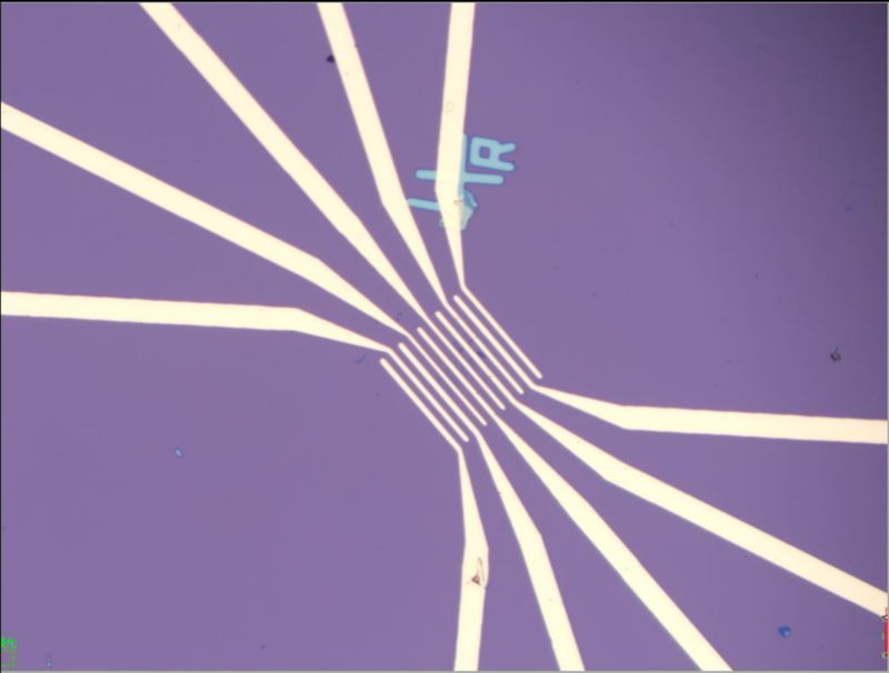
Lithography technology is mainly used in the manufacture of semiconductor devices and integrated circuits.
Process capability
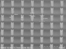
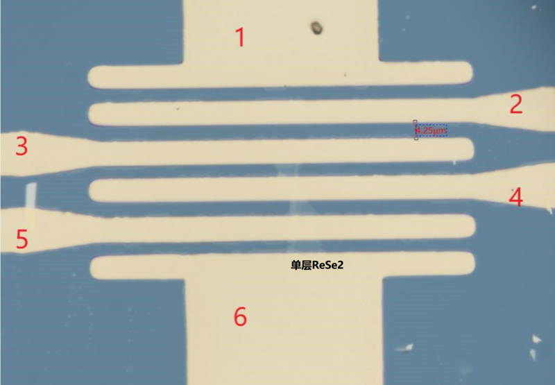
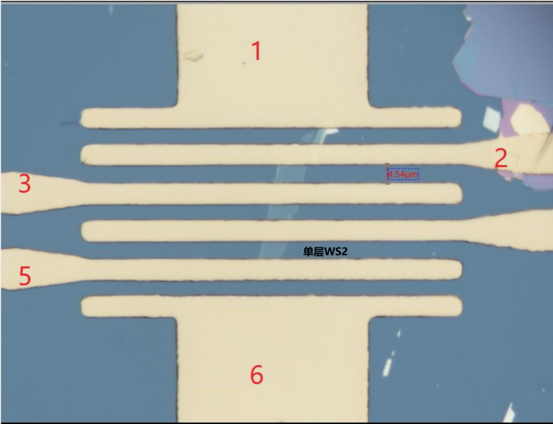
Electron beam lithography: The minimum line width is 50nm, and the accuracy can reach 10%. Step lithography: stepper i7 / i10 / i12, minimum line width 350nm, exposure error ± 0.1um, maximum exposure area 6 inches. Contact, proximity lithography: MA6 / BA6 lithography machine, minimum line width 1um, exposure error ± 0.5um
Our advantage
According to customer needs, customize the most cost-effective lithography solution High precision and small line width Substrate size range 1cm to 6 inches High-fidelity graphics
|
Warm tip: the products supplied by Beijing Beike Xincai Technology Co., Ltd. are only used for scientific research, not for human body |