registered   |   log in
  中文

北科产品中心 products center

MXenes-Max 2D transition metal carbonitride
MBene two-MAB-dimensional transition metal borides
MOFs metal organic framework compound
COFs covalent organic compound
Bioluminescent dyes
Aerogels
CVD TMDC 2D thin film / heterojunction
Perovskite material
Copper-doped modified lead apatite (LK 99 crystal powder)
2D material fiber/film
Two-dimensional material micro-nano processing - in situ testing
Basic magnetic beads, immunomagnetic beads, protein purification magnetic beads, nucleic acid extraction magnetic beads
Nucleic acid extraction kit
High-entropy materials
Biological nanomaterials
Nanocellulose
AIE luminescent material
Silane Bismuthene Borene Tellurene Phosphorene Graphyne
Binary CVD TMDC crystal/powder/dispersion
Ternary CVD TMDC crystal/powder/dispersion
Graphene and carbon nanomaterials
High-performance battery materials
Carbon nanotube/fullerene series
Nano/micron powder material and AAO template
Nanowires
Molecular sieve
Ionic liquid
QDS
Nanomaterial customization / material simulation calculation
Metal nanomaterials
Hydrogel Series and Consumables
Solid-state lithium battery
Product Solutions
Industrial-grade nanomaterials
Special materials for sodium storage
Thermoelectric materials
Organic materials
Atomic catalyst
Mesoporous materials
Heavy launch-new products are online!
Two-dimensional layered double hydroxide
catalyst
Nanosphere
Material testing and consumables
Inorganic Nanomaterials
equipment
MXenes 2D transition metal carbonitride
Detailed

Vacuum coating refers to the deposition of a metal or non-metal on the surface of the material in the form of a vapor in a vacuum environment to form a dense film. The quality of the coating is critical to the functional formation of semiconductor devices.

Technology application

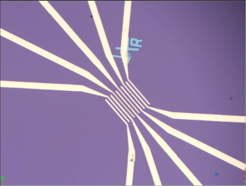
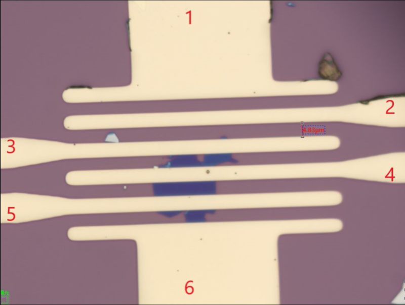
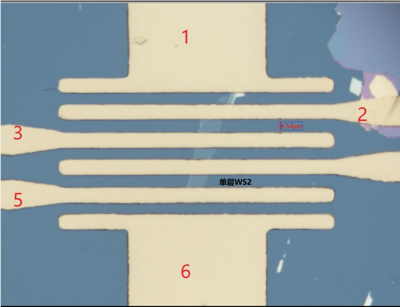
Coating technology is mainly used in the manufacturing process of micro-nano semiconductor devices. Metal and ITO materials are mainly used in the preparation of electrodes, and other non-metallic materials are mainly used in the preparation of insulating dielectric layers and sacrificial mask layers.

Process capability

Master coating technology:

Electron beam evaporation Magnetron sputtering LPCVD PECVD ALD

Coating material:

Metal: Ti, Al, Ni, Au, Ag, Cr, Pt, Cu, TiW90, Pd, Zn, Mo, W, Ta, Nb, etc. Non-metal: Si, SiO2, SiNx, Al2O3, HFO2, MgF2, ITO, Ta2O5, etc.

Coated substrate:

Silicon wafer, quartz glass wafer, sapphire wafer, PET, Pi, etc.

Our advantage

Master a variety of coating technologies and a wide range of coating materials Coating thickness range: 5nm-2000nm Base size 6 inches downward compatible The uniformity of the coating is good, and the coating is dense.


Warm tip: the products supplied by Beijing Beike Xincai Technology Co., Ltd. are only used for scientific research, not for human body

Message
Full name: *
Whatsapp/Wechat: *
E-mail: *
Contents:
 
Twitter:2D materials Frontier
QQ Exchange Group:1092348845


Reminder: Beijing Beike New Material Technology Co., Ltd. supplies products only for scientific research, not for humans
All rights reserved © 2019 beijing beike new material Technology Co., Ltd 京ICP备16054715-2号
advisory
phone
Email:mxenes@163.com
Tel:+86-17715390137
scan

scan
WeChat