

 Nanomedicine
ACS Nano | Engineered Nanodiamonds for Quantum Sensing: Nanoscale Material Limitations
QQ Academic Group: 1092348845
Detailed
 Optically addressable solid-state spin defects have become powerful multimodal quantum sensors, with nitrogen-vacancy (NV) centers in bulk diamond providing benchmark quantum control and sensitivity at room temperature. Embedding these defects into nanodiamonds (NDs) extends their capabilities to mobile probes that can access complex biological and nanoscale environments. However, reducing the size brings constraints beyond just bulk spin impurities, particularly enhanced lattice strain and surface-induced noise sources, which shorten NV spin relaxation times (T1 and T2), disrupt the NV charge state, and lead to significant particle-to-particle variations in nanodiamonds typically made by top-down methods. These effects complicate the sensing performance and the quantitative interpretation of multimodal signals in real environments. This paper provides a structured perspective on how material properties limit NV behavior in nanodiamonds through physical mechanisms and outlines mitigation strategies, laying the foundation for the robust use of these mobile quantum sensors in biosensing and nanoscale science.
Quick Look at Literature
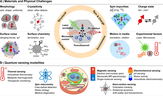
Figure 1.
Bottlenecks and sensing opportunities of nitrogen vacancy (NV) centers in nitrogen-doped diamonds (NDs). (a) When using NDs for NV-based quantum sensing, the main factors limiting their performance can be divided into four categories: structural disorder, surface-related effects, spin and charge-state control, and environmental influences. The schematic of the center shows an ND containing an NV center, where the core sensing principle relies on optical initialization of the NV spin and photoluminescence (PL) readout, with microwave control applied when needed. (b) Representative sensing opportunities enabled by NDs highlight their role as mobile probes in complex biological and nanoscale environments.
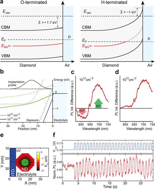
Figure 2 shows NV charge state control through surface electrostatics and electrochemical modulation. (a) Schematic band diagram of oxygen-terminated and hydrogen-terminated diamond surfaces in contact with air or water, showing the vacuum level (Evac), electron affinity (χ), band bending, conduction band minimum (CBM), valence band maximum (VBM), Fermi level (EF) alignment with environmental chemical potential (μ), and NV⁰/⁻ charge transition level (E_NV⁰/⁻). (b–d) Simulated band diagrams of hydrogen-terminated diamond for two nitrogen ion implantation doses (10¹² and 10¹³ cm⁻²), showing the implantation profile and depth-dependent alignment of VBM (solid line) and NV charge transition levels (NV⁺/⁰, dashed line; NV⁰/⁻, dotted line), along with photoluminescence difference spectra under electrochemical gating (+0.5 V and −0.5 V). Adapted with permission from reference (94). (e,f) Simulated 2D maps of VBM near the ITO/ND interface, highlighting regions where E_NV⁰/⁻ < EF (green) to stabilize NV⁻; corresponding photoluminescence measurements show voltage-induced modulation of NV charge states in single NV centers in ND ensembles. Adapted with permission from reference (95).
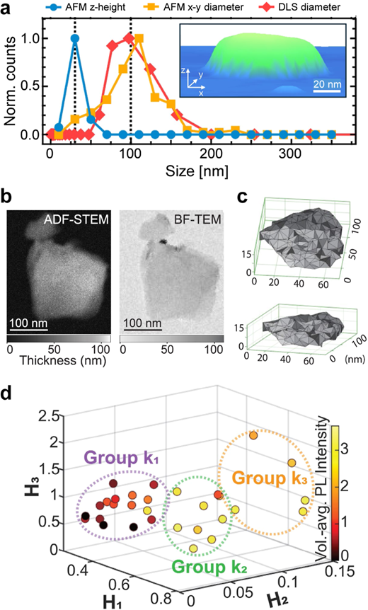
Figure 3
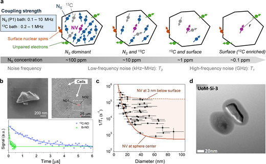
Figure 4
Noise sources and spin relaxation of diamond nitrogen-vacancy centers. (a) Schematic showing how the main magnetic noise mechanisms change with the concentration of substitutional nitrogen ([NS]). The NV-surface distance r highlights the strong distance dependence of surface-related noise. Typical magnetic interaction strengths and the characteristic frequency ranges controlling T1 and T2 relaxation are also indicated. (b) Scanning electron microscope image of 12C-rich diamond nanoparticles (high NV density), corresponding optical microscope image of nanoparticles internalized in cells, and representative T2 spin echo decay compared to Ib-type nanoparticles. Adapted from reference (37), under CC BY 4.0 license. (c) Particle size-dependent T1 relaxation rates of Ib-type nanoparticles, along with spherical model simulations for a single NV located at the particle center or 3 nm below the surface, showing the dominant role of surface-induced magnetic noise in small particles. Adapted from reference (26), with permission. Copyright American Physical Society. (d) Transmission electron microscope image of silica-coated nanoparticles used to reduce surface-related noise. Reprinted with permission from reference (40). Copyright 2025 American Chemical Society. UoM-Si-3 indicates the sample name.
Reference Info
ACS Nano (IF 17.3) Pub Date: 2026-6-09, DOI: 10.1021/acsnano.6c03795
We specialize in custom nano-medical functional materials. We conduct targeted development to tailor structure, particle size and surface modification for your experiments. Full characterization, iterative optimization and technical support are available for targeted delivery, bioimaging and nanomedicine studies. Send your evaluation plans to us.
Engineer Zhang: 17715390137
Engineer Chen: 18914047343
- Previous: Bone Immunity Idea | A
- Next: Frontiers of Medical E


