I. Overview of the article.
MXenes is a prominent family of two-dimensional materials because of their metal conductivity and rich surface functions.Although diene as bulk particles has been widely studied or independent thin films, thin films and transparent thin films needed for optical, optoelectronic, sensing and other applications. In this study, the author demonstrated a simple method to fabricate ultra-thin 10nm and Ti3C2TxMXene thin films by interfacial assembly technology. The self-assembly behavior of MXene thin films results in high stacking order and strong plane adhesion, in which the best thin film with 10nm thickness shows a low sheet resistance of 310 Ω / -.Using surface tension, the film is transferred to various types of flat and curved substrates. In addition, a number of thin films are continuously transferred from a batch of solution to the substrate, indicating the effective use of the material.When the thin film is used as a gas sensing channel, a signal-to-noise ratio as high as 320 is observed. Among them, the gas response of the thin film assembled from the small sheet of MXene is 10 times higher than that of the thin sheet assembled from large thin sheet.
Second, guided reading of picture and text.
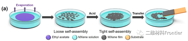
Figure 1.
Schematic diagram of interface self-assembly for the fabrication of ultra-thin (nanometer) MXene films.
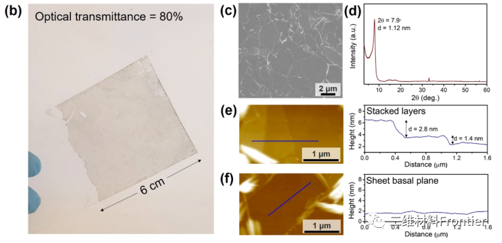
Figure 2.
A large area (6×6cm2) of the Ti3C2 is transmitted to a digital image on a PET substrate.
In this paper, the author proposes that the small interlayer distance may be due to two reasons: first, it can be derived from highly ordered superposition and good plane adhesion, which is known to reduce the interlaminar spacing of two-dimensional laminates; second, the undissolved ethyl acetate molecules in MXene interlayers may be easier to evaporate than water during vacuum annealing, allowing a smaller interlayer spacing between MXene layers than single layer water. In order to further study the packing direction and uniformity of the thin films, atomic force microscope (AFM) measurements were carried out. Figure e shows the area of the film, where the sheets are stacked evenly to form a ladder shape.

Figure 3.
The floating MXene film is statically transferred to a cylindrical substrate.
Instructions for transferring MXene films to curved substrates using static and dynamic transfer methods. For further development, two different transmission methods are designed, namely static conversion and dynamic transmission. Static transfer is a typical and direct method, in which the floating film on the surface is transferred vertically to the substrate. In the transfer method, the exact area of the floating membrane corresponds to the area of the target substrate.
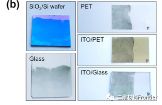
Figure 4.
High resolution TEM image of Ti3C2Tx.
Using this transfer method, we can transfer MXene films to different substrates. Static transfer method is used to transfer Ti3C2 thin films to planar substrates, such as SiO2/Si wafer, glass, PET and so on. Since the thin film has been assembled on the water interface before the transfer by this method, compared with the traditional method, the pretreatment of the substrate is not important, and the properties of the substrate (hydrophilicity, roughness, etc.) play an important role in obtaining uniform thin films.
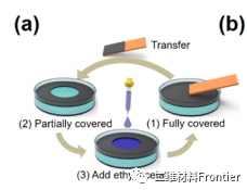
Figure 5.
Iterative process diagram for the preparation of multiple MXene films from a single batch of MXene solution.
The transfer of the MXene film from the fully covered surface to the target substrate results in a floating MXene film with partial area coverage. Then, a few drops of ethyl acetate were added to the uncovered area, and the self-assembly process was resumed with a new MXene sheet. In further iterations, no further hydrochloric acid was added to minimize the aggregation of MXene sheets.
III. Summary of the full text.
Transfer the assembled film to various substrates, including surfaces that reduce the radius of curvature to 1mm. At the same time, it is proved that the material can be used efficiently, that is, several MXene thin films are assembled sequentially, and multiple MXene thin films are transferred repeatedly from a single batch of MXene solution with a solution concentration of 0.1mg/mL. These films are further used as gas sensors to show their excellent performance in thin film devices. The authors expect that this method is suitable for thin films other than Ti3C2 and allows thin films to be fabricated on complex surfaces for a variety of applications.
This information is from the Internet for academic exchange only. if there is any infringement, please contact us to delete it immediately.