(Nanowerk Spotlight) Organic-inorganic metal halide perovskite has become a promising optoelectronic material with excellent structure and performance tunability. The new generation of functional materials has excellent properties such as large light absorption, long carrier diffusion length, high carrier mobility and low cost solution production process.
Ever since metal organic halide perovskite was reported as a visible light sensitizer for photovoltaic cells in 2009, research attention on metal halide perovskite has grown exponentially (JACS, "Organic metal halide perovskite as visible light for photovoltaic cells Sensitizer ").
In the following decade, rapidly developing research has applied perovskites to solar cells, photodetectors, light emitting diodes, and lasers.
In recent years, structural control of organic-inorganic metal halide hybrids has been explored to reduce the 3D size to 2D, 1D, and 0D at the morphological and molecular level (for example: "Ultra-thin perovskite nanocrystals, suitable for (Tunable and tunable). Energy-saving LEDs or work on luminescent nano-antennas based on halide perovskites).
At the same time, manufacturing methods based on inkjet printing have emerged to pattern the microstructure and nanostructure of perovskite. However, these perovskite patterning techniques are still limited to in-plane manufacturing and alignment.
To overcome this limitation, researchers have developed a method to print perovskite nanostructures in three dimensions. This method uses a soaring meniscus precursor ink formed on a nanopipette to locate and guide the solution-mediated perovskite crystallization in the air, thereby achieving nanoscale and free-form 3D printing.
Researchers led by the Department of Mechanical Engineering at the University of Hong Kong published their findings in "Advanced Materials" ("3D Nanoprinting of Perovskites").

Perovskite 3D printing
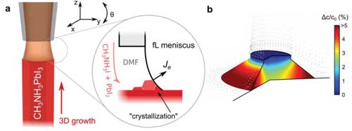
Perovskite 3D printing. a) Schematic showing 3D printing of a meniscus-guided organic-inorganic metal halide perovskite. The crystallization of CH 3 NH 3 PbI 3 occurs on a limited soaring (fL) ink meniscus, and its continuous guidance process enables nanoscale 3D printing. Inset: The evaporation loss of the solvent (J e: the evaporation flux of the solvent) increases the solute concentration on the meniscus surface and promotes the crystallization of the perovskite. b) The calculated concentration of perovskite solutes in the meniscus (height: 250 nm; wetting diameter: 1160 nm), forming an edge-shaped concentration field. The evaporation flux of the solvent is shown by the arrow. (Reprinted with permission from Wiley-VCH Verlag) (click on the image to enlarge)
As shown above, the perovskite crystals inside the meniscus of the fL ink are driven by the rapid evaporation of the DMF solvent. As shown in the illustration, at a given steady-state geometry of the fL meniscus, the evaporation loss of the solvent directly increases the concentration of the perovskite solute on the meniscus surface because the solute does not evaporate into the air.
The researchers explained that controlling crystallization in three dimensions is based on moving the nanopipette with a motorized platform (see video below): "When a nanometer pipette filled with ink with a diameter of 600 nm approaches and physically contacts the Si substrate At this time, the fL volume of ink was formed on the substrate wetted by the meniscus in the gap between the pipette substrates. Three crystals of CH 3 NH 3 lead iodide immediately began to grow in the liquid surface of the ink.
They described the 3D printing process. He said, "As the pipette moves upward (or the substrate moves downward) at a constant pulling speed, the crystal growth is guided by the pipette��s continuous ink supply in three directions. "" The termination of growth is performed by suddenly increasing the pulling speed above the threshold speed, so that the size of the freestanding perovskite nanowires can be adjusted in situ. "
Drawing speed is the central factor controlling the growth of perovskite nanowires. In addition, the precise drawing process can control the internal structure of the nanowires (see the figure below). Evaporation-driven transport of perovskite solutes depends on the size of the meniscus controlled by the pipette pull. Specifically, the hollowness of the perovskite nanowires from the tubular to the solid shape can be directly controlled by the instant change in the drawing speed of the pipette.

Growth kinetics of 3D printed perovskite nanowires. The internal structure of the perovskite nanowires can also be adjusted by ��. As �� increases, the internal structure changes from a hollow shape to a solid shape due to a decrease in the inner diameter ID. At 50% RH, as �� increases, both OD (round) and ID (square) decrease. Inset: FE-SEM images showing cross-sections (scale bar: 1 ��m) of perovskite nanowires obtained with different pulling speeds. (Reprinted with permission from Wiley-VCH Verlag)
After preparing and characterizing free-standing CH 3 NH 3 PbI 3 perovskite nanowires at a single entity level, the research team turned their attention to free-form 3D printing guided by an omnidirectional meniscus.
The production of the mesh structure is the first step towards a layer-by-layer additive manufacturing process. By using a 90 �� tilted nanopipette to laterally guide the ink meniscus, researchers have proven the reliable manufacture of the perovskite network structure.

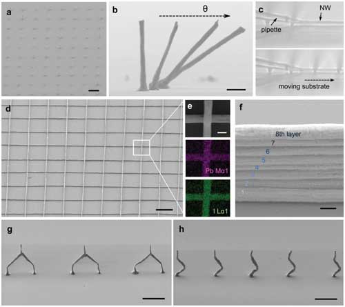
3D perovskite building. a) Vertical array of perovskite nanowires (scale bar: 20 ��m). b) Inclined perovskite nanowires are made by changing the angle of the pipette to the substrate (scale bar: 5 ��m). c�Ce) Making a mesh structure. c) An optical microscope image showing the horizontal printing process by tilting the pipette by 90 ��. d) FE-SEM image of perovskite network structure (scale bar: 20 ��m). e) Magnified FE-SEM and EDX images of perovskite nanojunctions (scale bar: 1 ��m). f) Perovskite nanowalls, stacked in eight layers (scale bar: 1 ��m). g) Independent curved knots (scale bar: 10 ��m). h) Vertical serpentine structure (scale bar: 10 ��m). (Reprinted with permission from Wiley-VCH Verlag) (click on the image to enlarge)
The author concludes: "The superior ability of this method to tailor the size of nanostructures in an on-demand, minimalist way can help to scientifically base the foundations of perovskite-based devices such as nanolasers, photodetectors and metasurfaces Research. "" If a comprehensive study of printing parameters affecting evaporation-induced crystallization can be completed, this method can be used to produce free-form perovskite nanostructures with programmed chemical composition. "
By Michael Berger - Michael is the author of three books of the Royal Society of Chemistry: Nano Association: push the boundaries of technology, nanotechnology: the future is tiny, and nano-engineering: techniques and tools manufacturing technology invisible Copyright © Nanowerk


