【introduction】
Ultra-thin two-dimensional semiconductor layered materials are believed to effectively extend Moore‘s Law of integrated circuit transistors. The key challenge currently facing 2D semiconductors is how to avoid the formation of charge scattering and trap sites in adjacent dielectrics. More and more studies have shown that the insulating van der Waals layer of hexagonal boron nitride (hBN) can provide excellent interfacial dielectric properties while effectively reducing charge scattering. However, how to achieve reliable single crystal hexagonal boron nitride thin film growth on wafers has become a technical difficulty that must be tackled in the industry.
[Achievement Profile]
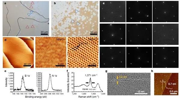
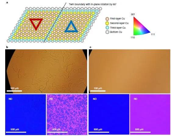
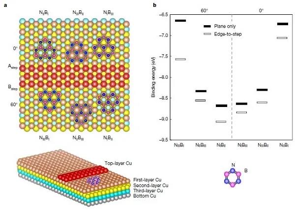
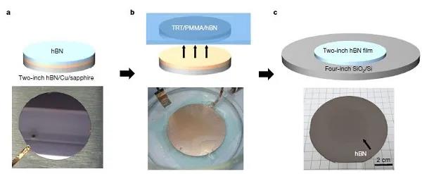
Wen-Hao Chang of National Chiao Tung University in Taiwan, Lain-Jong Li of TSMC, and BI Yakobson (co-corresponding author) of Rice University in the United States have jointly reported on the successful epitaxial growth of single crystal hexagons on sapphire wafer Boron nitride single layer. Previous theories have suggested that a hexagonal boron nitride single layer cannot achieve unidirectional growth on a highly symmetrical copper (111) metal surface. However, researchers have unexpectedly discovered that after lateral docking of hexagonal boron nitride with copper (111), the epitaxial growth of hexagonal boron nitride can be enhanced and the epitaxial growth is guaranteed to be unidirectional. The study also found that the single crystal hexagonal boron nitride thus prepared can be integrated between molybdenum disulfide and hafnium dioxide as an interface layer, which can greatly enhance the electrical performance of the transistor. The study believes that this method, which can be used to produce wafer-level single crystal hexagonal boron nitride, lays the foundation for the realization of new two-dimensional electronic devices. On March 04, 2020, related results were published online in Nature with an article entitled "Wafer-scale single-crystal hexagonal boron nitride monolayers on Cu (111)".
[Picture and text guide]


Literature link: Wafer-scale single-crystal hexagonal boron nitride monolayers on Cu (111) (Nature, 2020, DOI: 10.1038 / s41586-020-2009-2)


