(Nanowerk Spotlight) Despite the recent surge in research into the development of new structures and materials such as organic and perovskite, inorganic crystalline silicon solar cells still account for more than 90% of the market.
The reasons why most commercial solar cells use crystalline silicon as the absorbing layer include long-term stability, the abundance of silicone, relatively low manufacturing costs, the ability to be doped with other elements, and the passivation layer of natural oxides.
However, the indirect band gap properties of crystalline silicon make it a poor light emitter, which limits its solar conversion efficiency. For example, compared to the extraordinary high light absorption coefficient of perovskite, silicon requires more than 1,000 times more material to absorb the same amount of sunlight.
In order to reduce the cost per watt of the next generation solar cell and increase the utilization rate per gram, reducing the thickness of the active absorber is a key design requirement. This is where new two-dimensional (2D) materials like graphene come into play because they can lead to thinner, lighter and more flexible solar cells.
To date, several experimental designs of graphene-based solar cells have been reported, where graphene is used as a different part of the cell.
Due to its excellent electron transport properties and extremely high carrier mobility, not only graphene, but also other direct band-gap monolayer materials such as transition metal dihalides (TMDC) and black phosphorus, also show great potential, Can be used for low cost, flexibility and flammability. Efficient photovoltaic equipment.
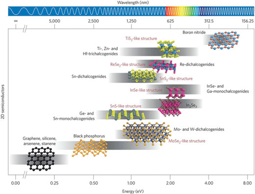
Comparison of band gap values of different 2D semiconductor material series. The crystal structure is also shown to highlight similarities and differences between different families. Gray horizontal bars indicate the range of band gap values that can be crossed by changing the number of layers, strain or alloying. All of these 2D semiconductors have wide bandgap ranges that can be used in a variety of photonics and optoelectronics applications such as thermal imaging, fiber optic communications, photovoltaics, displays, and light emitting diodes. (© Springer Nature) (click image to enlarge)
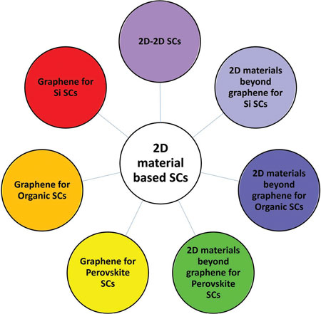
A recent review of advanced materials ("The role of graphene and other 2D materials in solar photovoltaics") provides a comprehensive overview of current 2D materials-based solar photovoltaic technologies. It describes the latest advances in graphene, graphene-based materials, and other 2D materials for solar photovoltaics, including silicon-based solar cells, organic perovskite solar cells.
Graphene-based solar cells
In their first review, the authors described the role of doped and undoped graphene as ultra-thin transparent conductive electrodes and Schottky barrier junction layers (hole collectors) for silicon-based solar cells. This section also discusses graphene (undoped / doped) as a charge transport layer / transparent electrode for organic / perovskite solar cells.
In solar cells, the electric field formed by the potential energy barrier between two different materials at the interface can separate electrons and holes, which are generated by the absorption of light in the material. According to the type of material at the interface, there are three types of junctions: homojunction, heterojunction (formed between two different semiconductors with different band gaps), and Schottky junction (with band bending Metal-semiconductor junction).
Although graphene can better transmit light into semiconductors, it can also form a Schottky barrier junction with silicon to effectively separate electron-hole pairs and collect charge carriers. The author discusses in detail the role of graphene as a transparent conductive electrode and a junction layer (hole collector) in graphene-Si solar cells.
ITO has a key role as a transparent conductive electrode of organic-based and perovskite-based solar cells, but has some disadvantages. In these organic solar cells, graphene (due to its high electrical conductivity, required work function, and optimal surface morphology) can be a potential alternative to ITO, while at the same time transparency, conductivity, flexibility, higher materials Utilization and performance provide similar performance. Reduce processing costs.
This review comprehensively covers the role of graphene-based materials in ternary materials for electrodes, charge transport layers, and organic solar cells, as well as charge transport layers and stabilization materials for perovskite solar cells.
Schematics of different types of 2D-based solar cells. (Reprinted with permission from Wiley-VCH Verlag)
The role of 2D materials in solar cell applications other than graphene
In theory, a single TMDC single layer with sub-nanometer thickness has the ability to absorb up to 50 nm of Si or 15 nm of gallium arsenide (GaAs) sunlight, so it can generate up to 4.5 mA cm -2 current.
The authors discuss and calculate the potential performance of TDMC in silicon-based solar cells, organic solar cells, and perovskite solar cells.
The concept of ultra-thin 2D / 2D heterojunction solar cells
The author states: "From a photovoltaic perspective, the idea of full two-dimensional solar cells seems to be less effective because the conventionally used active materials are much thicker and absorb more sunlight. But, interestingly, this solar energy Cells have the potential to surpass the performance of traditional Si and GaAs-based photovoltaic cells. TMDC has an energy gap in the visible to near-infrared spectrum, which makes it very suitable for solar cell applications. "
"Furthermore, because they are direct-bandgap semiconductors with a single layer thickness, they have high radiation efficiency. This combined with their significantly higher absorption coefficient per unit thickness (greater than Si, GaAs and perovskite) makes them The strong absorption of high absorptive ultra-thin photovoltaic devices in thin atomic layers with sharp, clean interfaces enables the highest wattage / gram utilization of active materials. "
Next generation 2D photovoltaic
In the final part of this article, next-generation concepts such as tandem and hot-load solar cells based on 2D materials, and on-chip integrated designs for energy collection and storage devices are discussed, resulting in an ideal solar cell that absorbs the energy of any absorbed photons .
Finally, the authors provide a brief outlook on meeting the challenges and requirements of next-generation 2D photovoltaics at low cost and high productivity. "We believe graphene has shown tremendous research and industrial potential and can be incorporated into standard technology roadmaps for photovoltaics. To this end, a worrying issue is that graphene must compete with existing processes and supply chains for existing materials , Such as silicon and indium tin. However, we believe that materials with great potential should always complement and complement each other, not compete with each other. "
Source: Nanowerk