Detailed consultation with customer service
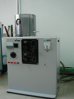
Ion thinning
Ion thinning instrument is a special tool of transmission electron microscope, which is used to prepare samples with large area of electron penetration area.
External services:
1. It is mainly used for preparing thin film samples of TEM;
2. It can be used to prepare microscope transmission samples of metal, nonmetal, semiconductor, ceramic, rock and other solid materials;
3. Ion thinning at low and normal temperature.
Carbon spraying
Vacuum evaporation carbon film (carbon spraying) vacuum evaporation, gold, silver, nickel, aluminum and other metals.
Focused ion beam system (FIB)
Focused ion beam system (FIB): sample preparation of micro nano structure of materials, including: TEM sample preparation under SEM on-line observation, material micro section cutting and observation, sample micro etching and deposition, etc.
Zeiss Auriga focused ion beam field emission scanning double beam electron microscopy
Focused ion beam field emission scanning double beam electron microscopy (FIB) is an advanced equipment for nanostructure analysis and preparation of materials. It is equipped with electron beam and GA ion beam, which can realize the simultaneous on-line observation of electron beam and ion beam. It has the characteristics of stable beam flow, high resolution and precise nano manipulation. It can observe and analyze the three-dimensional, high-quality and high stability micro shape, crystal structure and phase structure of materials under the resolution of nano scale, as well as the qualitative chemical composition of various materials micro areas And quantitative detection.
The main technical indicators:
SEM Resolution: 1.0nm @ 15kV 1.9nm @ 1kV
Magnification mag.: 12 ~ 1000000x
Accelerating voltage EHT:0.1 ~ 30kV
FIB resolution: 2.5nm @ 30KV
Magnification mag.: 300 ×~ 500000 ×
Acceleration voltage eht: 1.0 ~ 30KV
Configure configuration
Detector: inlens secondary electronic detector
E-T secondary electronic detector
ESB back scattering electron detector
X-ray spectrometer
Resolution: 127 EV @ MNK α
Detection range of elements: be (4) ~ FM (100)
EBSD detector
Spatial resolution: 50nm
Main functions:
1. Field emission scanning electron microscopy (SEM): morphology observation and analysis of various materials, such as metals, semiconductors, ceramics, polymer materials, organic polymers, etc
2. EDS: composition analysis of material micro area; half width of mnka peak is better than 127ev; half width of CKA peak is better than 56ev; half width of FKA peak is better than 64ev; element be4-u92;
3. 3D EBSD: crystal orientation and texture analysis and 3D reconstruction of polycrystalline materials; spatial resolution: better than 50nm; detector sensitivity: when the accelerating voltage is 3KV, the beam current is less than 50pA, and the pattern can be collected; the resolution speed can reach up to 600 points / S; the simultaneous acquisition and integration function of test energy spectrum and EBSD are tested, and the actual samples are selected to enter Three dimensional EDS & EBSD test was performed
4. Focused ion beam system (FIB): sample preparation of material micro nano structure, including: TEM sample preparation under SEM online observation, material micro section cutting and observation, sample micro etching and deposition, etc.
|
Warm tip: the products supplied by Beijing Beike Xincai Technology Co., Ltd. are only used for scientific research, not for human body |
| Item ID |
CAS |
ID |
Pack |
Parameter |
Stock |
Make up |
Price |
| BK2020011702-01 |
|
BK2020011702 |
|
离子减薄 |
100 |
|
$0 |
| BK2020011702-02 |
|
BK2020011702 |
|
喷碳 |
100 |
|
$0 |
| BK2020011702-03 |
|
BK2020011702 |
|
聚焦离子束系统(FIB) |
100 |
|
$0 |