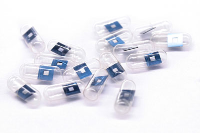
Suzhou Beike Nano Technology Co., Ltd. specializes in the production and processing of copper mesh used in transmission electron microscopes, which is the carrier mesh for carrying samples. If the carrier net is made of copper, it is called copper net; if it is nickel, molybdenum, gold, or nylon, it is called nickel net, molybdenum net, gold net, nylon net, etc. accordingly. The carrier net series is specially designed and produced for transmission electron microscope (TEM). At the same time, it also provides special network for other scientific research fields. Divided into square holes, round holes, apertures, slits, parallel, double, and other special carrier nets, etc., it can meet the scientific research needs of materials, biology and many disciplines. At the same time, it acts as an agent to sell the network of imported brands from the United States, the United Kingdom, and Japan.
When purchasing carbon support film, which mesh of copper mesh support film is suitable. Under normal circumstances, for nanomaterials, 300 mesh or 230 mesh copper mesh carbon support film is more suitable; for biological materials (slice samples), 200 mesh or 150 mesh copper mesh carbon support film is more suitable.
If you are using nano-materials (below 50nm) and you want to look at high-resolution images, it is recommended to choose a microgate film; if you are using nano-materials (below 10nm), the sample dispersion is very good, and it is recommended to use an ultra-thin carbon support film. But the premise is to use a high-resolution electron microscope (above 200kV). If you are using a 100kV electron microscope, it is not necessary to choose a microgate film.
◆ What is the difference between copper mesh, carbon support film, micro grid, ultra-thin carbon film, and porous film?
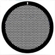
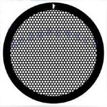
▲ Copper mesh is usually the copper mesh used for transmission electron microscopy, which is the carrier mesh for carrying samples. If the carrier net is made of copper, it is called copper net; if it is nickel, molybdenum, gold, or nylon, it is called nickel net, molybdenum net, gold net, and nylon net accordingly. Copper mesh is also called "bare mesh". Mainly used in biological sample preparation, it can be used with a slicer to collect samples in a sink with a "naked net". Then carry out carbon spray treatment, and then enter the electron microscope observation.
▲ Carbon support film When preparing samples for most TEM samples, in order to ensure that the sample can be mounted on the "carrier net", a layer of organic film is covered on the "carrier net", called the "support film". This kind of carrier net with supporting film is called "carrier net supporting film". When the sample comes into contact with the carrier mesh supporting film, it will be firmly adsorbed on the supporting film and will not slip off the holes of the carrier mesh. In order to observe on the electron microscope.
When the sample is placed in an electron microscope, the "reticulated support film" will be irradiated by electron beams, and charge accumulation will occur on the organic support film, which will also cause the sample to discharge, causing the sample to float, jump, and rupture the support film. Therefore, people consider spraying carbon on the support film to improve the conductivity of the support film and achieve a good observation effect. This "carbon-sprayed grid support film", referred to as "carbon support film", generally has a film thickness of 10-20nm.
From the perspective of production cost and use effect, copper mesh is the most economical and practical, so it is widely used. Therefore, the frequently mentioned "copper mesh support film", "carbon support film", "carbon film", "fanghua film", etc., and even the misnamed "copper mesh", mostly refer to the Net spray carbon support film". Usually called "carbon support film".
▲Micro grid support film Micro grid is a kind of support film. It is a micro-hole specially made in the film when the support film is made, so it is also called "micro grid support film". It is also a carbon sprayed support film. Generally the film thickness is 15-30nm. It is mainly to enable the sample to be mounted on the edge of the micropore of the support film so that the sample can be observed "without film". The purpose of no film is mainly to improve image contrast.
Therefore, to observe tubular, rod-shaped, nano-agglomerates, etc., the "micro-gate" support film is often used, and the effect is very good. Especially when observing high-resolution images of these samples, it is a good choice.
In the test, the commonly used carbon support film and small hole micro grid are commonly used to collect samples. In fact, there is an ultra-thin carbon film on the small hole micro grid. For high-resolution shots, the thickness of the sample should be controlled below 20nm, so generally powders with a diameter less than 20nm are directly picked up, and the larger the particles, the thinning of the ions after embedding.
▲ Ultra-thin carbon film is also a kind of support film. It is on the basis of the micro grid, superimposed with a very thin carbon film, generally 3-5nm. The purpose of this ultra-thin carbon film is to block the micropores with a thin carbon film. Since the micro-grid has a better observation effect, why should the hole be blocked? This is mainly for those nanomaterials with good dispersibility, such as samples below 10nm, and samples with good dispersibility.
▲Porous carbon support film It is a product with common characteristics of ordinary carbon support film and microgate support film. Ordinary carbon support film is mainly used for observing morphology and rubbing dispersion, while microgate support film is mainly for viewing high resolution. Since the porous membrane has a larger supporting membrane area and occasional micropores on the membrane, it is possible to obtain both the dispersibility of nanoparticles and the acquisition of topography and high-resolution images. It is a very practical support film product.
◆To observe the high resolution of nanotubes with different lengths, which film is best to choose?
There are generally two purposes for watching nanotubes. One is to look at the length, mainly to observe at low magnification; the other is to look at the tube wall, mainly to look at the high-magnification image.
Regardless of the length, as long as you look at high magnification images, especially high resolution, it is best to use a micro-gate film or a porous film. It can not only meet the observation length of low magnification, but also meet the requirements of high resolution observation. But you must choose "High Resolution Transmission Electron Microscope" (HRTEM), otherwise, your microgate film will be difficult to function. Under normal circumstances, a good "carbon support film" can also see the high-resolution image of the carbon nanotube wall, but it must not exceed the effect of observation with the "micro gate film".
The reason is: there are holes in the micro-gate film, and the tube wall can be observed at the holes of the micro-gate, while the carbon support film has no holes, and the background of the film will affect the high-resolution observation. The same goes for powder samples.
◆What kind of copper mesh support film is suitable for observing nano materials and biological materials?
When purchasing carbon support film for the first time, it is often not known which mesh copper mesh support film is suitable. Under normal circumstances, for nanomaterials, 300 mesh or 230 mesh copper mesh carbon support film is more suitable; for biological materials (slice samples), 200 mesh or 150 mesh copper mesh carbon support film is more suitable.
If you are using nano-materials (below 50nm) and you want to look at high-resolution images, it is recommended to choose a microgate film; if you are using nano-materials (below 10nm), the sample dispersion is very good, and it is recommended to use an ultra-thin carbon support film. But the premise is to use a high-resolution electron microscope (above 200kV). If you are using a 100kV electron microscope, it is not necessary to choose a microgate film
|
Warm tip: the products supplied by Beijing Beike Xincai Technology Co., Ltd. are only used for scientific research, not for human body |
| Item ID |
CAS |
ID |
Pack |
Parameter |
Stock |
Make up |
Price |
| BK2020122801-01 |
|
BK2020122801 |
|
100目/100枚 |
100 |
|
$206 |
| BK2020122801-02 |
|
BK2020122801 |
|
400目/100枚 |
100 |
|
$188 |
| BK2020122801-03 |
|
BK2020122801 |
|
200目/100枚 |
100 |
|
$169 |
| BK2020122801-04 |
|
BK2020122801 |
|
300目/100枚 |
100 |
|
$169 |
| BK2020122801-05 |
|
BK2020122801 |
|
超薄碳膜50枚 |
100 |
|
$282 |
| BK2020122801-06 |
|
BK2020122801 |
|
双联网200目50枚 |
100 |
|
$154 |
| BK2020122801-07 |
|
BK2020122801 |
|
微栅200目50枚 |
100 |
|
$225 |
| BK2020122801-08 |
|
BK2020122801 |
|
100目/50枚 |
100 |
|
$105 |
| BK2020122801-09 |
|
BK2020122801 |
|
200目/50枚 |
100 |
|
$102 |
| BK2020122801-10 |
|
BK2020122801 |
|
300目/50枚 |
100 |
|
$102 |
| BK2020122801-11 |
|
BK2020122801 |
|
400目/50枚 |
100 |
|
$105 |
| BK2020122801-12 |
|
BK2020122801 |
|
微栅300目50枚 |
100 |
|
$225 |
| BK2020122801-13 |
|
BK2020122801 |
|
纯碳膜50枚 |
100 |
|
$135 |
| BK2020122801-14 |
|
BK2020122801 |
|
裸铜网50枚 |
100 |
|
$38 |
| BK2020122801-15 |
|
BK2020122801 |
|
230目50枚 |
100 |
|
$102 |
| BK2020122801-16 |
|
BK2020122801 |
|
方华膜50枚 |
100 |
|
$132 |
| BK2020122801-17 |
|
BK2020122801 |
|
200/300目镍网碳膜50枚 |
100 |
|
$206 |
| BK2020122801-18 |
|
BK2020122801 |
|
200/300目镍网方华膜50枚 |
100 |
|
$244 |
| BK2020122801-19 |
|
BK2020122801 |
|
200/300目金网碳膜50枚 |
100 |
|
$263 |
| BK2020122801-20 |
|
BK2020122801 |
|
坐标载网碳膜F1、F2 100枚 |
100 |
|
$488 |