Detailed consultation with customer service
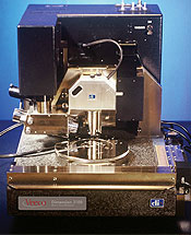
AFM atomic force microscope
The atomic force microscope (AFM) uses the micro cantilever to sense and amplify the force between the tip probe on the cantilever and the atom of the sample under test, so as to achieve the purpose of detection, with the resolution of atomic level. Because AFM can observe both conductor and non conductor, it makes up for the deficiency of STM.
Compared with SEM, AFM has many advantages. Unlike electron microscopy, which can only provide two-dimensional images, AFM provides real three-dimensional surface images. At the same time, AFM does not need any special treatment of the sample, such as copper plating or carbon, which will cause irreversible damage to the sample. Thirdly, the electron microscope needs to operate in high vacuum, and the AFM can work well under atmospheric pressure or even in liquid environment. In this way, it can be used to study biological macro molecules and even living biological tissues. Compared with scanning tunneling microscope (STM), AFM has more extensive applicability because it can observe non-conductive samples. The scanning force microscope, which is widely used in scientific research and industry, is based on the atomic force microscope.
Compared with scanning electron microscope (SEM), AFM has the disadvantages of too small imaging range, slow imaging speed and too large influence of probe.
Atomic force microscope of Di company
The surface properties of semiconductor wafers, etch masks, magnetic media, CD / DVD, biomaterials, optical materials and other samples with a diameter of up to 200 mm can be measured by using automatic AFM and STM technology.
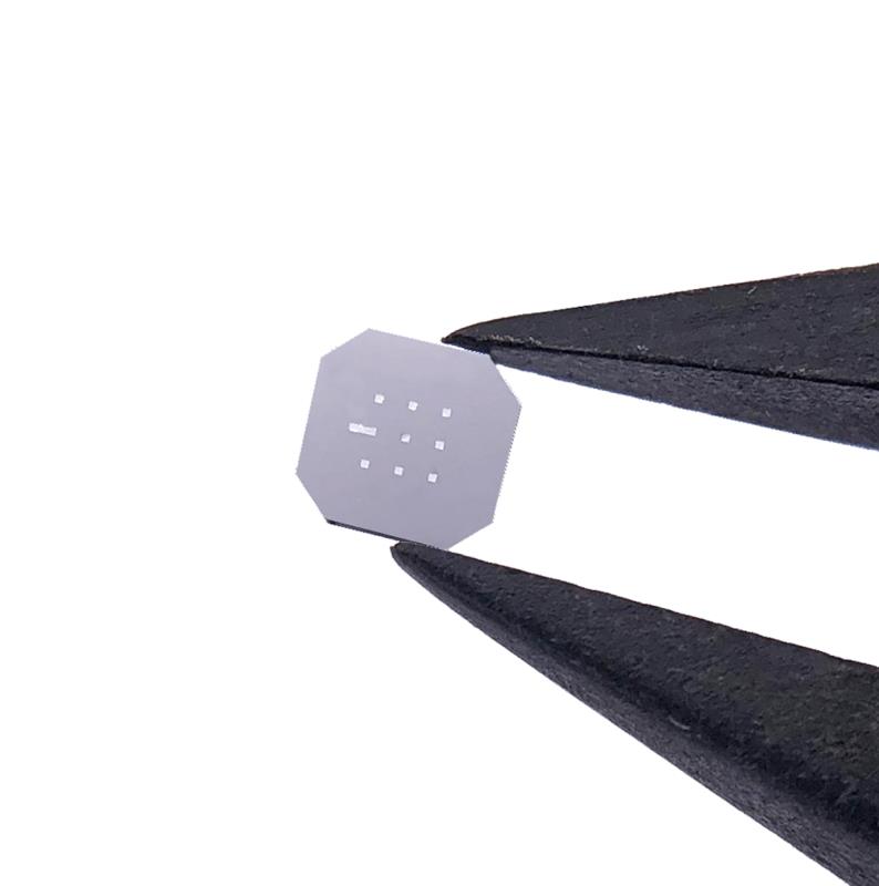
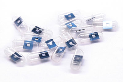
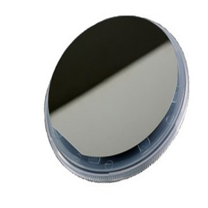
The objects of AFM research can be organic solids, polymers and biomacromolecules, etc. the carrier selection of samples is very wide, including mica, glass, graphite, polished silicon, silicon dioxide and some biofilms, among which the most commonly used is the newly peeled mica, the main reason is that it is very flat and easy to handle. The best way to polish silicon wafer is to boil it for 1 h at 90 ℃ in 7:3 mixture of concentrated sulfuric acid and 30% hydrogen peroxide. The carrier with good conductivity, such as graphite or the substrate plated with metal, is needed for the test of electrical properties.
The thickness of the specimen, including the thickness of the specimen table, is 10 mm maximum. If the sample is too heavy, sometimes it will affect the action of scanner, please do not let the heavy sample go. The size of the specimen shall be no larger than the size of the specimen table (diameter 20 mm). It‘s OK to be a little bigger. However, the maximum value is about 40 mm. If the measurement is not fixed properly, displacement may occur. Please fix it before measuring.
Indentation test
N2100 nanoindentation instrument in USA
1. The mechanical properties of various coatings, films, ultrafilms, organic polymer films, biomembranes, multilayer composite films, DLC films, lubricating films, heterogeneous materials, semiconductor materials, MEMS, biomaterials and related industrial products can be effectively studied and evaluated by indentation test;
2. Mechanical data such as hardness, rigidity, modulus of elasticity, fracture strength, failure point, stress-strain and creep were measured.
In-situ fatigue
Sem-servo high temperature in situ fatigue testing machine
Tensile test: maximum load ≤ 1.3kn (error 1n); maximum displacement 10 m m (error 1 μ m)
Tension tension fatigue test: maximum dynamic load ≤ 1kn; maximum frequency ≤ 10Hz (variable frequency during test)
Test temperature: room temperature ~ 800 ℃ (vacuum)
Magnification: x50-x200000, and the effective magnification under dynamic test conditions is 5000 times.
External services:
(1) SEM microstructure observation
(2) Tensile and fatigue test
(3) The changes of surface morphology and microstructure, as well as the initiation and propagation of cracks were observed in real time
Sample size as shown in the figure (meet the maximum load)
|
Warm tip: the products supplied by Beijing Beike Xincai Technology Co., Ltd. are only used for scientific research, not for human body |
| Item ID |
CAS |
ID |
Pack |
Parameter |
Stock |
Make up |
Price |
| BK2020011701-01 |
|
BK2020011701 |
|
AFM原子力显微镜 |
100 |
|
$0 |
| BK2020011701-02 |
|
BK2020011701 |
|
压痕测试 |
100 |
|
$0 |
| BK2020011701-03 |
|
BK2020011701 |
|
原位疲劳 |
100 |
|
$0 |